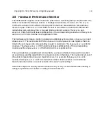
The E31 core has a(n) 2-way set-associative 16 KiB L1 instruction cache and a(n) 16 KiB L1
DTIM.
All cores have Physical Memory Protection (PMP) units.
The Level 1 memories are described in Chapter 3. The PMP is described in Section 3.7.
The AON block contains the reset logic for the chip, an on-chip low-frequency oscillator, a
watchdog timer, connections for an off-chip low-frequency oscillator, the real-time clock, a pro-
grammable power-management unit, and 32×32-bit backup registers that retain state while the
rest of the chip is in a low-power mode.
The AON can be instructed to put the system to sleep. The AON can be programmed to exit
sleep mode on a real-time clock interrupt or when the external digital wakeup pin,
dwakeup_n
, is
pulled low. The
dwakeup_n
input supports wired-OR connections of multiple wakeup sources.
The Always-On block is described in Chapter 13.
The GPIO complex manages the connection of digital I/O pads to digital peripherals, including
SPI, UART, I²C, and PWM controllers, as well as for regular programmed I/O operations.
The GPIO complex is described in more detail in Chapter 17.
Universal Asynchronous Receiver/Transmitter
Multiple universal asynchronous receiver/transmitter (UARTs) are available and provide a
means for serial communication between the FE310-G002 and off-chip devices.
The UART peripherals are described in Chapter 18.
Hardware Serial Peripheral Interface (SPI)
There are 3 serial peripheral interface (SPI) controllers. Each controller provides a means for
serial communication between the FE310-G002 and off-chip devices, like quad-SPI Flash mem-
ory. Each controller supports master-only operation over single-lane, dual-lane, and quad-lane
protocols. Each controller supports burst reads of 32 bytes over TileLink to accelerate instruc-
tion cache refills. 1 SPI controller can be programmed to support eXecute-In-Place (XIP) modes
to reduce SPI command overhead on instruction cache refills.
Copyright © 2019, SiFive Inc. All rights reserved.
11
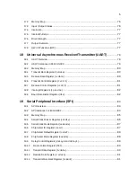
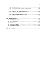
Содержание FE310-G002
Страница 1: ...SiFive FE310 G002 Manual v19p05 SiFive Inc ...
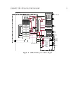
Страница 11: ...Figure 1 FE310 G002 top level block diagram Copyright 2019 SiFive Inc All rights reserved 9 ...
Страница 15: ...Chapter 2 List of Abbreviations and Terms 13 ...
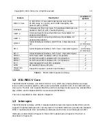
Страница 23: ...Chapter 4 Memory Map The memory map of the FE310 G002 is shown in Table 4 21 ...


