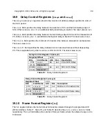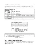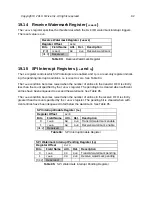
The
delay0
and
delay1
registers allow for the insertion of arbitrary delays specified in units of
one SCK period.
The
cssck
field specifies the delay between the assertion of CS and the first leading edge of
SCK. When
sckmode.pha
= 0, an additional half-period delay is implicit. The reset value is
0x1
.
The
sckcs
field specifies the delay between the last trailing edge of SCK and the deassertion of
CS. When
sckmode.pha
= 1, an additional half-period delay is implicit. The reset value is
0x1
.
The
intercs
field specifies the minimum CS inactive time between deassertion and assertion.
The reset value is
0x1
.
The
interxfr
field specifies the delay between two consecutive frames without deasserting
CS. This is applicable only when
sckmode
is HOLD or OFF. The reset value is
0x0
.
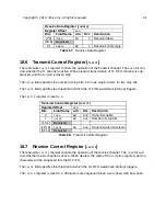
Delay Control Register 0 (
delay0
)
Register Offset
0x28
Bits
Field Name
Attr.
Rst.
Description
[7:0]
cssck
RW
0x1
CS to SCK Delay
[15:8]
Reserved
[23:16]
sckcs
RW
0x1
SCK to CS Delay
[31:24]
Reserved
Delay Control Register 1 (
delay1
)
Register Offset
0x2C
Bits
Field Name
Attr.
Rst.
Description
[7:0]
intercs
RW
0x1
Minimum CS inactive time
[15:8]
Reserved
[23:16]
interxfr
RW
0x0
Maximum interframe delay
[31:24]
Reserved
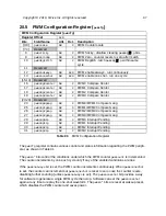
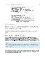
The
fmt
register defines the frame format for transfers initiated through the programmed-I/O
(FIFO) interface. Table 77, Table 78, and Table 79 describe the
proto
,
endian
, and
dir
fields,
respectively. The
len
field defines the number of bits per frame, where the allowed range is 0 to
8 inclusive.
Table 74:
Delay Control Register 0
Table 75:
Delay Control Register 1
Copyright © 2019, SiFive Inc. All rights reserved.
89
Содержание FE310-G002
Страница 1: ...SiFive FE310 G002 Manual v19p05 SiFive Inc ...
Страница 11: ...Figure 1 FE310 G002 top level block diagram Copyright 2019 SiFive Inc All rights reserved 9 ...
Страница 15: ...Chapter 2 List of Abbreviations and Terms 13 ...
Страница 23: ...Chapter 4 Memory Map The memory map of the FE310 G002 is shown in Table 4 21 ...

