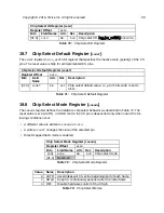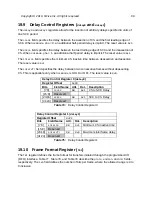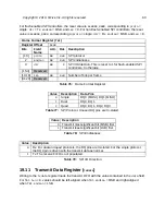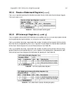
The
rxmark
register specifies the threshold at which the Rx FIFO watermark interrupt triggers.
The reset value is
0x0
.
Receive Watermark Register (
rxmark
)
Register Offset
0x54
Bits
Field Name
Attr.
Rst.
Description
[2:0]
rxmark
RW
0x0
Receive watermark
[31:3]
Reserved
The
ie
register controls which SPI interrupts are enabled, and
ip
is a read-only register indicat-
ing the pending interrupt conditions.
ie
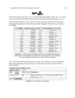
is reset to zero. See Table 84.
The
txwm
condition becomes raised when the number of entries in the transmit FIFO is strictly
less than the count specified by the
txmark
register. The pending bit is cleared when sufficient
entries have been enqueued to exceed the watermark. See Table 85.
The
rxwm
condition becomes raised when the number of entries in the receive FIFO is strictly
greater than the count specified by the
rxmark
register. The pending bit is cleared when suffi-
cient entries have been dequeued to fall below the watermark. See Table 85.
SPI Interrupt Enable Register (
ie
)
Register Offset
0x70
Bits
Field Name
Attr.
Rst.
Description
0
txwm
RW
0x0
Transmit watermark enable
1
rxwm
RW
0x0
Receive watermark enable
[31:2]
Reserved
SPI Watermark Interrupt Pending Register (
ip
)
Register Offset
0x74
Bits
Field Name
Attr.
Rst.
Description
0
txwm
RO
0x0
Transmit watermark pending
1
rxwm
RO
0x0
Receive watermark pending
[31:2]
Reserved
Table 83:
Receive Watermark Register
Table 84:
SPI Interrupt Enable Register
Table 85:
SPI Watermark Interrupt Pending Register
Copyright © 2019, SiFive Inc. All rights reserved.
92
Содержание FE310-G002
Страница 1: ...SiFive FE310 G002 Manual v19p05 SiFive Inc ...
Страница 11: ...Figure 1 FE310 G002 top level block diagram Copyright 2019 SiFive Inc All rights reserved 9 ...
Страница 15: ...Chapter 2 List of Abbreviations and Terms 13 ...
Страница 23: ...Chapter 4 Memory Map The memory map of the FE310 G002 is shown in Table 4 21 ...

