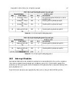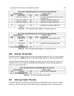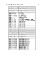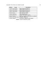
PLIC Interrupt Pending Register 1 (
pending1
)
Base Address
0x0C00_1000
Bits
Field Name
Attr.
Rst.
Description
0
Interrupt 0 Pend-
ing
RO
0
Non-existent global interrupt 0 is hard-
wired to zero
1
Interrupt 1 Pend-
ing
RO
0
Pending bit for global interrupt 1
2
Interrupt 2 Pend-
ing
RO
0
Pending bit for global interrupt 2
…
31
Interrupt 31 Pend-
ing
RO
0
Pending bit for global interrupt 31
Table 28:
PLIC Interrupt Pending Register 1
PLIC Interrupt Pending Register 2 (
pending2
)
Base Address
0x0C00_1004
Bits
Field Name
Attr.
Rst.
Description
0
Interrupt 32 Pend-
ing
RO
0
Pending bit for global interrupt 32
…
20
Interrupt 52 Pend-
ing
RO
0
Pending bit for global interrupt 52
[31:21]
Reserved
WIRI
X
Table 29:
PLIC Interrupt Pending Register 2
Each global interrupt can be enabled by setting the corresponding bit in the
enables
registers.
The
enables
registers are accessed as a contiguous array of 2 × 32-bit words, packed the
same way as the
pending
bits. Bit 0 of enable word 0 represents the non-existent interrupt ID 0
and is hardwired to 0.
Only 32-bit word accesses are supported by the
enables
array in SiFive RV32 systems.
Copyright © 2019, SiFive Inc. All rights reserved.
47
Содержание FE310-G002
Страница 1: ...SiFive FE310 G002 Manual v19p05 SiFive Inc ...
Страница 11: ...Figure 1 FE310 G002 top level block diagram Copyright 2019 SiFive Inc All rights reserved 9 ...
Страница 15: ...Chapter 2 List of Abbreviations and Terms 13 ...
Страница 23: ...Chapter 4 Memory Map The memory map of the FE310 G002 is shown in Table 4 21 ...

