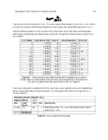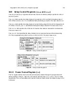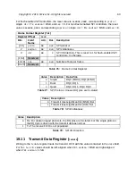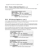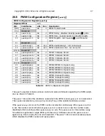
The input clock is the bus clock
tlclk
. The reset value of the register is set to
div_init
, which
is tuned to provide a 115200 baud output out of reset given the expected frequency of
tlclk
.
Table 62 shows divisors for some common core clock rates and commonly used baud rates.
Note that the table shows the divide ratios, which are one greater than the value stored in the
div
register.
tlclk
(MHz)
Target Baud (Hz)
Divisor
Actual Baud (Hz)
Error (%)
2
31250
64
31250
0
2
115200
17
117647
2.1
16
31250
512
31250
0
16
115200
139
115107
0.08
16
250000
64
250000
0
200
31250
6400
31250
0
200
115200
1736
115207
0.0064
200
250000
800
250000
0
200
1843200
109
1834862
0.45
384
31250
12288
31250
0
384
115200
3333
115211
0.01
384
250000
1536
250000
0
384
1843200
208
1846153
0.16
Table 62:
Common baud rates (MIDI=31250, DMX=250000) and required
divide values to achieve them with given bus clock frequencies. The divide val-
ues are one greater than the value stored in the
div
register.
The receive channel is sampled at 16× the baud rate, and a majority vote over 3 neighboring
bits is used to determine the received value. For this reason, the divisor must be ≥16 for a
receive channel.
Baud Rate Divisor Register (
div
)
Register Offset
0x18
Bits
Field
Name
Attr.
Rst.
Description
[15:0]
div
RW
X
Baud rate divisor.
div_width
bits wide, and the reset
value is
div_init
.
[31:16]
Reserved
Table 63:
Baud Rate Divisor Register
Copyright © 2019, SiFive Inc. All rights reserved.
83
Содержание FE310-G002
Страница 1: ...SiFive FE310 G002 Manual v19p05 SiFive Inc ...
Страница 11: ...Figure 1 FE310 G002 top level block diagram Copyright 2019 SiFive Inc All rights reserved 9 ...
Страница 15: ...Chapter 2 List of Abbreviations and Terms 13 ...
Страница 23: ...Chapter 4 Memory Map The memory map of the FE310 G002 is shown in Table 4 21 ...


