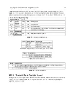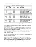
PWM 2 Compare Register (
pwmcmp2
)
Register Offset
0x28
Bits
Field Name
Attr.
Rst.
Description
[15:0]
pwmcmp2
RW
X
PWM 2 Compare Value
[31:16]
Reserved
PWM 3 Compare Register (
pwmcmp3
)
Register Offset
0x2C
Bits
Field Name
Attr.
Rst.
Description
[15:0]
pwmcmp3
RW
X
PWM 3 Compare Value
[31:16]
Reserved
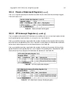
The primary use of the
ncmp
PWM compare registers is to define the edges of the PWM wave-
forms within the PWM cycle.
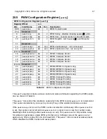
Each compare register is a
cmpwdith
-bit value against which the current
pwms
value is com-
pared every cycle. The output of each comparator is high whenever the value of
pwms
is greater
than or equal to the corresponding
pwmcmp
.
If the
pwmzerocomp
bit is set, when
pwms
reaches or exceeds
pwmcmp0
,
pwmcount
is cleared to
zero and the current PWM cycle is completed. Otherwise, the counter is allowed to wrap
around.
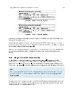
To avoid glitches in the PWM waveforms when changing
pwmcmp
register values, the
pwmdeglitch
bit in
pwmcfg
can be set to capture any high output of a PWM comparator in a
sticky bit (
pwmcmp
ip
for comparator
) and prevent the output falling again within the same
PWM cycle. The
pwmcmp
ip
bits are only allowed to change at the start of the next PWM cycle.
Note
The
pwmcmp0ip
bit will only be high for one cycle when
pwmdeglitch
and
pwmzerocmp
are
set where
pwmcmp0
is used to define the PWM cycle, but can be used as a regular PWM
edge otherwise.
If
pwmdeglitch
is set, but
pwmzerocmp
is clear, the deglitch circuit is still operational but is now
triggered when
pwms
contains all 1s and will cause a carry out of the high bit of the
pwms
incre-
menter just before the counter wraps to zero.
Table 95:
PWM 2 Compare Register
Table 96:
PWM 3 Compare Register
Copyright © 2019, SiFive Inc. All rights reserved.
99
Содержание FE310-G002
Страница 1: ...SiFive FE310 G002 Manual v19p05 SiFive Inc ...
Страница 11: ...Figure 1 FE310 G002 top level block diagram Copyright 2019 SiFive Inc All rights reserved 9 ...
Страница 15: ...Chapter 2 List of Abbreviations and Terms 13 ...
Страница 23: ...Chapter 4 Memory Map The memory map of the FE310 G002 is shown in Table 4 21 ...

