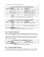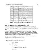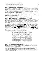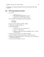
Source Start
Source End
Source
1
1
AON Watchdog
2
2
AON RTC
3
3
UART0
4
4
UART1
5
5
QSPI0
6
6
SPI1
7
7
SPI2
8
39
GPIO
40
43
PWM0
44
47
PWM1
48
51
PWM2
52
52
I2C
Table 26:
PLIC Interrupt Source Mapping
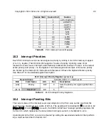
Each PLIC interrupt source can be assigned a priority by writing to its 32-bit memory-mapped
priority
register. The FE310-G002 supports 7 levels of priority. A priority value of 0 is
reserved to mean "never interrupt" and effectively disables the interrupt. Priority 1 is the lowest
active priority, and priority 7 is the highest. Ties between global interrupts of the same priority
are broken by the Interrupt ID; interrupts with the lowest ID have the highest effective priority.
See Table 27 for the detailed register description.
PLIC Interrupt Priority Register (
priority
)
Base Address
0x0C0 4 × Interrupt ID
Bits
Field Name
Attr.
Rst.
Description
[2:0]
Priority
RW
X
Sets the priority for a given global inter-
rupt.
[31:3]
Reserved
RO
0
Table 27:
PLIC Interrupt Priority Registers
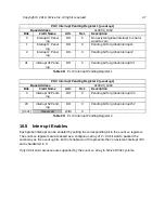
The current status of the interrupt source pending bits in the PLIC core can be read from the
pending array, organized as 2 words of 32 bits. The pending bit for interrupt ID
is stored in bit
of word
. As such, the FE310-G002 has 2 interrupt pending registers. Bit
0 of word 0, which represents the non-existent interrupt source 0, is hardwired to zero.
A pending bit in the PLIC core can be cleared by setting the associated enable bit then perform-
ing a claim as described in Section 10.7.
Copyright © 2019, SiFive Inc. All rights reserved.
46
Содержание FE310-G002
Страница 1: ...SiFive FE310 G002 Manual v19p05 SiFive Inc ...
Страница 11: ...Figure 1 FE310 G002 top level block diagram Copyright 2019 SiFive Inc All rights reserved 9 ...
Страница 15: ...Chapter 2 List of Abbreviations and Terms 13 ...
Страница 23: ...Chapter 4 Memory Map The memory map of the FE310 G002 is shown in Table 4 21 ...

