5
List Of Tables
Table 5: Binary Preset Speed Select
Table 6: Progressive Preset Speed Operation
Table 7: Programmable Output Selections
Table 11: Binary Input Control
Table 12: Progressive Input Control
Table 13: Fault Code Descriptions
Table 14: Connector Definitions
Table 15: Test Point Definitions
Table 16: SCR Gate Resistance Testing
List Of Figures
Figure 1: DSD 412 Block Diagram A
Figure 2: DSD 412 Block Diagram B
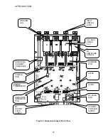
Figure 3: Component Layout Front View
Figure 4: Component Layout Right Side View
Figure 5: Common Problems in Encoder Mounting
Figure 6: Typical Power Wiring
Figure 7: Typical Analog Signal Wiring
Figure 8: Typical Serial Signal Wiring
Figure 9: Power/ Signal Wiring Notes
Figure 10: Drive Brake Control Feature
Figure 11: Speed Select Logic Input Wiring
Figure 12: S-Curve Accel/Decel Cycle
Figure 13: S-Curve Accel with min %S
Figure 14: S-Curve with 100% S
Figure 15: E-REG Tracking Profiles (1)
Figure 16: E-REG Tracking Profiles (2)
Figure 17: E-REG Tracking Profiles (3)
Figure 19: Elevator Start - Stop Timing
Figure 20: Analog Signal Ground Noise
Figure 21: Serial Link Connections
Figure 22: Other Faulting Conditions
Figure 23: I/O Monitor Function
Figure 24: Connector and E-prom Locations
Figure 25: Test Point Locations
Figure 26: Drive Chassis Outline, DSD 412, 100 Amp
Figure 27: Drive Chassis Outline, DSD 412, 195 Amp
Figure 28: Drive Chasis Outline, DSD 412, 300 Amp
Figure 29: Layout, DSD 412, 100 Amp
Figure 30: Layout, DSD 412, 195 Amp
Figure 31: Layout, DSD 412, 300 Amp
Содержание DSD 412
Страница 1: ...DSD 412 DC Elevator Drive Technical Manual CS00407 rev 06...
Страница 6: ...6...
Страница 102: ...MAINTENANCE 102 Figure 24 Connector and E prom Locations...
Страница 103: ...MAINTENANCE 103 Figure 25 Test Point Locations...
Страница 115: ...OUTLINE DRAWING 100A 115 Figure 26 Drive Chassis Outline DSD 412 100 Amp...
Страница 116: ...OUTLINE DRAWING 190A 116 Figure 27 Drive Chassis Outline DSD 412 195 Amp...
Страница 117: ...OUTLINE DRAWING 300A 117 Figure 28 Drive Chasis Outline DSD 412 300 Amp...
Страница 118: ...LAYOUT DRAWING 100A 118 Figure 29 Layout DSD 412 100 Amp A3 A1 A2 A2 L1 NEG GND L2 L3 POS...
Страница 119: ...LAYOUT DRAWING 195A 119 Figure 30 Layout DSD 412 195 Amp A3 A1 A2 A2...
Страница 120: ...LAYOUT DRAWING 300A 120 Figure 31 Layout DSD 412 300 Amp A3 A1 A2 A2...
Страница 121: ......


