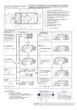
ACLK
SMCLK
SMCLK
00
01
10
11
UCSSELx
UCLKI
(1)
Prescaler/Divider
Bit Clock Generator
UCxBRx
16
BRCLK
Transmit Shift Register
UCMST
I2C State Machine
Receive Shift Register
UCA10 UCGCEN
UCxSDA
UCxSCL
UCSLA10
Address Mask
UCBxADDMASK
Byte Counter UCBxBCNT
Own Address
UCBxI2COA0
Receive Buffer UCBxRXBUF
Transmit Buffer UCBxTXBUF
Slave Address UCBxI2CSA
Own Address
UCBxI2COA1
Own Address
UCBxI2COA2
Own Address
UCBxI2COA3
(1)
(2)
Externally provided clock on the eUSCI_B SPI clock input pin
Not the actual implementation (transistor not located in eUSCI_B module)
(2)
(2)
Clock Low
timeout generator
MODCLK
eUSCI_B Operation – I
2
C Mode
1081
SLAU208Q – June 2008 – Revised March 2018
Copyright © 2008–2018, Texas Instruments Incorporated
Enhanced Universal Serial Communication Interface (eUSCI) – I
2
C Mode
Figure 41-1. eUSCI_B Block Diagram – I
2
C Mode
41.3 eUSCI_B Operation – I
2
C Mode
The I
2
C mode supports any slave or master I
2
C-compatible device.
shows an example of an
I
2
C bus. Each I
2
C device is recognized by a unique address and can operate as either a transmitter or a
receiver. A device connected to the I
2
C bus can be considered as the master or the slave when
performing data transfers. A master initiates a data transfer and generates the clock signal SCL. Any
device addressed by a master is considered a slave.
I
2
C data is communicated using the serial data (SDA) pin and the serial clock (SCL) pin. Both SDA and
SCL are bidirectional and must be connected to a positive supply voltage using a pullup resistor.