


2. Signal Descriptions > JTAG Interface Signals
19
PEB383 User Manual
July 25, 2011
Integrated Device Technology, Inc.
Confidential - NDA Required
2.5
JTAG Interface Signals
2.6
Power-up Signals
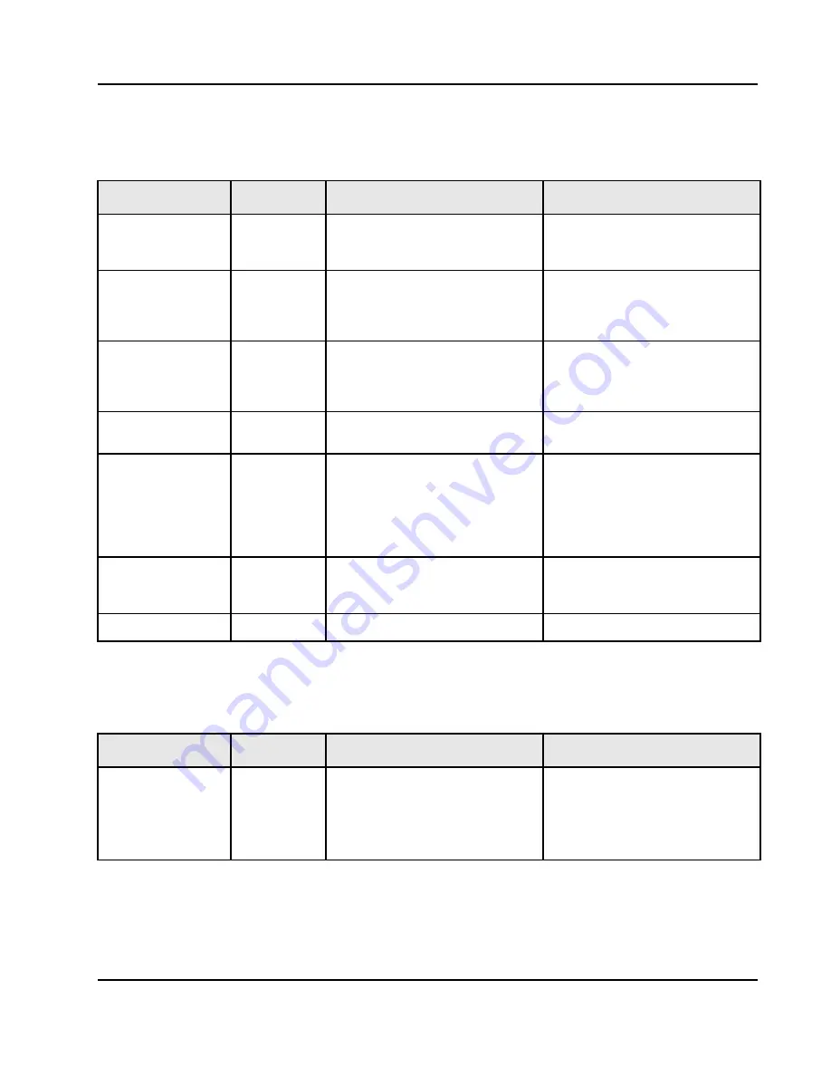
Table 5: JTAG Interface Signals
Name
Pin Type
Description
Design Recommendation
JTAG_TCK
3.3 In
Test Clock. This signal clocks state
information and data into and out of the
PEB383 during boundary scan.
Connect to 3.3V using a 2K pull-up
resistor.
JTAG_TDI
3.3 In PU
Test Data Input. This signal, in
conjunction with JTAG_TCK, shifts data
and instructions into the TAP controller
in a serial bit stream.
Connect to 3.3V using a 2K pull-up
resistor.
JTAG_TDO
3.3 Out
Test Data Output. This signal, in
conjunction with JTAG_TCK, shifts data
and instructions from the TAP controller
in a serial bit stream.
If JTAG is not used, leave unconnected.
JTAG_TMS
3.3 In PU
Test Mode Set. This signal controls the
state of the TAP controller.
Connect to 3.3V using a 2K pull-up
resistor.
JTAG_TRSTn
3.3 In PU
Test Reset. This signal forces the TAP
controller into an initialized state. This
signal must be pulsed or pulled low
externally to reset the TAP controller.
If JTAG is not used, connect this pin to a
2K pull-down resistor. If JTAG is used,
connect to output of AND gate where
inputs are TRST# and PERST#.
For more information, see the
PEB383
Evaluation Board User Manual
.
TEST_BCE
3.3 In
Test Boundary Scan Compatibility
Enabled. This input aids 1149.6 testing
and Scope function of PHYs.
For
1149.1
Boundary Scan testing, this
pin must be low. For
1149.6
Boundary
Scan testing, this pin must be high.
TEST_ON
3.3 In
This signal controls scan shift enable.
Pull down for normal operation.
Table 6: Power-up Signals
Name
Pin Type
Description
Design Recommendation
PWRUP_PLL_
BYPASS
3.3 In
PLL bypass. This signal bypasses the
PLL in the PCI clock generation (see
0 = Normal operation
1 = PLL bypass
This signal should always be tied low.


