


> PCIe and SerDes Control and Status Registers
215
PEB383 User Manual
July 25, 2011
Integrated Device Technology, Inc.
Confidential - NDA Required
14.9.10
PCIe Clock Module Control and Status Registers
14.9.11
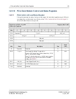
PCIe Control and Level Status Register
This register indicates the status of various control inputs. Its reset value depends on inputs. When its
accompanying override register is used, however (see
“PCIe Control and Level Override Register”
),
the relevant status bits are no longer valid.
Register name: PCIE_CTL_STAT
Reset value: Undefined
Register offset: 0x420
Bits
7
6
5
4
3
2
1
0
31
:
24
Reserved
TX_LVL
LOS_LVL
23
:
16
LOS_LVL
ACJT_LVL
15:08
Reserved
07:00
Reserved
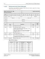
Bits
Name
Description
Type
Reset
Value
31
Reserved
Reserved
R
1
30:26
TX_LVL
Fine Resolution setting of Tx signal level.
Equation: Pk-Pk output level (without attenuation) = 1230 x
(48 + tx_lvl/2)/63.5 mV Vdiff-pp
Note: TX_LVL should be set to >= 0x1010 (which results in
an output of 1Vp-p). For more information on available
settings, see
R
0x10
25:21
LOS_LVL
Loss of Signal Detector level.
R
0x12
20:16
ACJT_LVL
AC JTAG Comparator level.
R
0x00
15:0
Reserved
Reserved
R
1


