


15. Electrical Characteristics > Power Supply Sequencing
221
PEB383 User Manual
July 25, 2011
Integrated Device Technology, Inc.
Confidential - NDA Required
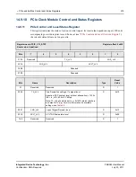
15.4
Power Supply Sequencing
The PEB383 does not have any power sequencing constraints.
15.5
DC Operating Characteristics
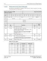
D3hot
L1
Power Saving Mode. All PCI Clocks
Gated
0.128
0.148
D3cold
N/A
Power Removed
0.060
0.069
Table 44: PEB383 Power Dissipation per Supply
Device
State
ASPM Link
State
Bridge Activity
Typical
Power
(W)
1.0V_A
(W)
3.3V_A
(W)
1.0V
(W)
3.3V
(W)
D0
L0
Fully Active Links
0.398
0.022
0.065
0.036
0.275
D0
L0
0% Link Activity
0.225
0.022
0.065
0.031
0.108
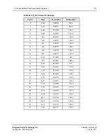
Table 45: DC Operating Characteristics
Symbol
Parameter
Condition
Minimum
Maximum
Units
Notes
V
OL_PCI
PCI Output Low Voltage
I
OL
= 1500uA
-
0.1V
DD_PCI
V
-
V
OH_PCI
PCI Output High
Voltage
I
OH
= -500uA
0.9V
DD_PCI
-
V
-
V
OH_33
3.3 CMOS Output High
Voltage
I
OH
= -6mA
V
DD_PCI
- 0.5
-
V
-
V
OL_33
3.3 CMOS Output Low
Voltage
I
OL
= 6mA
-
0.4
V
-
V
IH_33
3.3 CMOS Input High
Voltage
-
2
V
DD_PCI
+ 0.5
V
-
Table 43: PEB383 Power Dissipation
(Continued)
Device
State
ASPM Link
State
Bridge Activity
Typical
Power
(W)
Max
Power
(W)


