Detector System Component Description
50
Row 1
Row 2
Row 3
Row 4
Readout
Register
Col. 1
Col. 2
Col. 3
Col. 4
R1C1
R1C2
R1C3
R1C4
R2C1
R2C2
R2C3
R2C4
R3C1
R3C2
R3C3
R3C4
R4C1
R4C2
R4C3
R4C4
Empty Empty Empty Empty
Output
Amplifier
Storage
Output
Amplifier
Empty
Row 1
Row 2
Row 3
Row 4
Readout
Register
Col. 1
Col. 2
Col. 3
Col. 4
R1C1
R1C2
R1C3
R1C4
R2C1
R2C2
R2C3
R2C4
R3C1
R3C2
R3C3
R3C4
R4C1
R4C2
R4C3
R4C4
Empty Empty Empty Empty
Output
Amplifier
Storage
Output
Amplifier
Empty
Empty Empty Empty Empty
Plus
Plus
Plus
Plus
Starting Image
Two Shifts Down
(Verticle bin by 2)
Row 1
Row 2
Row 3
Row 4
Readout
Register
Col. 1
Col. 2
Col. 3
Col. 4
R1C1
R1C2
R1C3
R1C4
R2C1
R2C2
R2C3
R2C4
R3C1
R3C2
R4C1
R4C2
Empty Empty Empty Empty
Output
Amplifier
Storage
Output
Amplifier
Empty Empty Empty Empty
Plus
Plus
Plus
Two Shifts Across
(Horizontal bin by 2)
Empty Empty
R3C3+R4C3
R3C4+R4C4
Complete 2x2 Bin
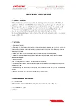
Figure 14.
Illustration of 2 x 2 Binning Operation on a 4 x 4 CCD Array
Summary of Contents for JOBIN YVON SYNAPSE
Page 1: ...SYNAPSE CCD Detection System User Manual Part Number 81100 Revision 2...
Page 10: ...Preface x...
Page 14: ...System Description and Specifications 4...
Page 28: ...Detector System Installation 18...
Page 38: ...Initial Power up and Operation 28...
Page 48: ...Temperature Control 38...
Page 72: ...Appendix A Dimensional Drawings 62 Figure 17 Distance from Focal Plane to CCD Chip...
Page 73: ...Appendix A Dimensional Drawings 63 Figure 18 Synapse Power Supply Unit...
Page 74: ...Appendix A Dimensional Drawings 64...
Page 86: ...Appendix C Performing Routine Procedures with SynerJY 76...
Page 100: ...Appendix E Accessories 90...
Page 104: ...Warranty 94...
Page 113: ...103 Notes...
Page 114: ...104 Notes...