


General Purpose Timer Module (GPT)
MCF52235 ColdFire® Integrated Microcontroller Reference Manual, Rev. 6
23-20
Freescale Semiconductor
3. Clear the pin’s DDR bit in PORTT
n
DDR.
4. Write to the OM
n
/OL
n
bits in GPTCTL1 to select the output action.
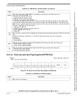
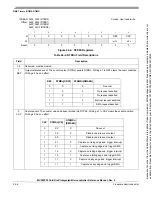
shows how various timer settings affect pin functionality.
Table 23-23. GPT Settings and Pin Functions
GPTEN DDR
1
1
When DDR set the pin as input (0), reading the data register returns the state of the pin. When DDR set the pin as output (1),
reading the data register returns the content of the data latch. Pin conditions such as rising or falling edges can trigger an
input capture on a pin configured as an input.
GPTIOS
EDGx
[B:A]
OMx/
OLx
2
2
OMn/OLn bit pairs select the output action to be taken as a result of a successful output compare. When OMn or OLn is set
and the IOSn bit is set, the pin is an output regardless of the state of the corresponding DDR bit.
OC3Mx
3
Pin
Data
Dir.
Pin
Driven
by
Pin
Function
Comments
0
0
X
4
X
X
X
In
Ext.
Digital input
GPT disabled by GPTEN = 0
0
1
X
X
X
X
Out
Data reg.
Digital output GPT disabled by GPTEN = 0
1
0
0 (IC)
0 (IC
disabled)
X
0
In
Ext.
Digital input
Input capture disabled by EDGn
setting
1
1
0
0
X
0
Out
Data reg.
Digital output Input capture disabled by EDGn
setting
1
0
0
<> 0
X
0
In
Ext.
IC and
digital input
Normal settings for input capture
1
1
0
<> 0
X
0
Out
Data reg.
Digital output Input capture of data driven to output
pin by CPU
1
0
0
<> 0
X
1
In
Ext.
IC and
digital input
OC3M setting has no effect because
IOS = 0
1
1
0
<> 0
X
1
Out
Data reg.
Digital output OC3M setting has no effect because
IOS = 0; input capture of data driven
to output pin by CPU
1
0
1 (OC)
X
(3)
0
5
0
In
Ext.
Digital input
Output compare takes place but
does not affect the pin because of
the OMn/OLn setting
1
1
1
X
0
0
Out
Data reg.
Digital output Output compare takes place but
does not affect the pin because of
the OMn/OLn setting
1
0
1
X
<> 0
0
Out
OC action
Output
compare
Pin readable only if DDR = 0
(5)
1
1
1
X
<> 0
0
Out
OC action
Output
compare
Pin driven by OC action
(5)
1
0
1
X
X
1
Out
OC action/
OC3Dn
Output
compare
(ch 3)
Pin readable only if DDR = 0
6
1
1
1
X
X
1
Out
OC action/
OC3Dn
Output
compare/
OC3Dn
(ch 3)
Pin driven by channel OC action and
OC3Dn via channel 3 OC
(6)
Because
of
an
order
from
the
United
States
International
Trade
Commission,
BGA-packaged
product
lines
and
part
numbers
indicated
here
currently
are
not
available
from
Freescale
for
import
or
sale
in
the
United
States
prior
to
September
2010:MCF52234CVM60,
MCF52235CVM60


