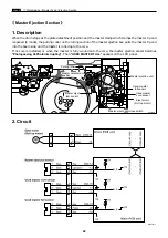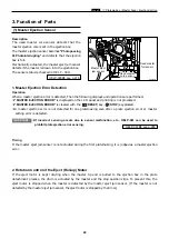
No.
Item
DP-S850
DP-S650 / S620
DP-S550 / S520 / S510
Specification
secondary scanning
primary scanning
600dpi (23.6 dots)
600dpi (23.6 dots)
34
z
Scanner Section
chap.2
(4) CCD / Lamp
Description
The lamp illuminates the document and the reflected light is transmitted onto the CCDs.The CCDs output
the image signals in level of voltage.
This machine adopts a xenon lamp which is lit quickly when turned on, and the quantity of light is
stable.The lamp is lit when the the control signal CN1-1 for the lamp inverter unit is LOW (0V) .
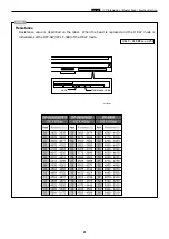
The table below shows the specification for the CCD.
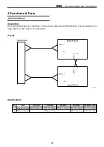
Circuit
• Lamp
• CCD
Specification
R8S02E05e
Optical signal storage time (SH cycle)
1
1.6 msec./ line
Frequency
2
5 MHz
The number of effective picture elements
3
7926 picture elements
Reading
density
5
Reading width
(This is not the image width
which can be processed.)
4
336 mm
1.6 msec./ line
5 MHz
5000 picture elements
400dpi (15.7 dots)
318 mm
400dpi (15.7 dots)
1.6 msec./ line
5 MHz
5000 picture elements
300dpi (11.8 dots)
318 mm
600dpi (23.6 dots)
Summary of Contents for DP-S Series
Page 1: ......
Page 9: ......
Page 11: ......
Page 16: ...x Dimensions chap 1 15 R8S01001 xDimensions 622 1360 510 228 1080 710 980 688 370 mm...
Page 22: ...v Part Names and Their Functions chap 1 21 44000A1e 2A 2B 2C R8S01006a 2Detailed drawing...
Page 33: ...32 z Scanner Section chap 2 Circuit R8S02E03e...
Page 87: ...86 m Drum Section chap 2 2 Circuit R8S02E30...
Page 171: ...170 MEMO...
Page 193: ...192 MEMO...
Page 195: ...194 z Help mode List chap 7 z HELP Mode List...
Page 243: ...242 c HELP Mode Function and Operation Procedures chap 7...
Page 270: ...269 c HELP Mode Function and Operation Procedures chap 7...
Page 281: ...280 MEMO...
Page 293: ...292 z Electrical Parts Layout and Their Functions chap 9 MEMO...
Page 295: ...309 294 x Overall Wiring Layout chap 9 Overall Wiring Layout 1 Main PCB 2 2...
Page 297: ...311 296 x Overall Wiring Layout chap 9 Overall Wiring Layout 2 Drive PCB 2 2...


