CMT2380F64
www. cmostek. com
Rev 0.3 | 50 / 83
is translated into dBm value after filtering.Users can read the register RSSI_CODE<7:0> to obtain the RSSI code value,or
RSSI_DBM<7:0> to obtain the dBm value. By setting the register RSSI_DET_SEL<1:0> Users can determine whetherthe RSSI is
output to the MCU in real time,or latched at the instance when the preamble,sync,or the whole packet is received.
Also,CMT2380F64 allows the user to setup a threshold by RSSI_TRIG_TH<7:0> to compare with the real-time RSSI value. If
the RSSI is larger than the threshold it outputs logic1, otherwise outputs logic 0. The output can be used as a source of the
RSSIVLD interrupt of the receive time extending condition in the super-low power (SLP)mode.
SAR
FILTER
CODE to dBm
CONVERT
SAR
ADC
RSSI AVG
FILTER
RSSI_CODE<7:0>
RSSI_DBM<7:0>
RSSI_AVG_MODE<2:0>
COMPARE to
RSSI_TRIG_TH<7:0>
RESULT
LATCH
LATCH
RSSI_DET_SEL<1:0>
RSSI_DET_SEL<1:0>
Figure
4-3.
RSSI detection and comparison circuit
CMT2380F64 has done a certain degree of calibration before delivery. In order to obtain more accurate RSSI measurement
results, the user needs to recalibrate the RSSI circuit in their dedicated applications. For further information, please refer to the
AN144-CMT2300A RSSI Usage Guideline.
4.8 Phase Jump Detector
(
PJD
)
PJD is Phase Jump Detector. When the chip is in FSK demodulation, it can automatically observe the phase jump characteristics
of the received signal to determine whether it is awanted signal or an unwanted noise.
2
SYM
2
SYM
1
SYM
1
SYM
1
SYM
1
SYM
Figure 4-4.
Received signal jump diagram
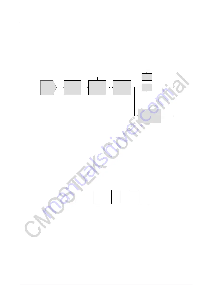
The PJD mechanism defines that the input signal switching from 0 to 1 or from 1 to 0 is a phase jump. Users can configure the
PJD_WIN_SEL<1:0> to determine the number of detected jumps for the PJD to identify a wanted signal. As shown in the above
figure, in total 8 symbols are received. But the phase jump only appeared 6 times. Therefore, the number of jumps is not equal to
the number of symbols. Only when a preamble is received they are equal. In general, the more jumps are used to identify the
signal, the more reliable the result is; the less jumps are used, the faster the result is obtained. If the RX timeis set to are latively
short period, it is necessary to reduce the number of jumps to meet the timing requirements. Normally, 4 jumps allow pretty
reliable result, e.g.the chip will not mistakenly treat an incoming noise as a wanted signal, and vice versa will not treat a wanted
signal as noise.
Detecting the phase jump of a signal, is identical to detect whether the signal is the expected data rate. In fact, at the same time,
the PJD will also detect the FSK deviation and see if it is valid, as well as to see if the SNR is over 7 dB. According to detect
result of the data rate and the Deviation as well as SNR, if it is detected as a reliable signal, it outputs logic 1, otherwise
outputs logic 0. The output can be used as a source of the RSSI VLD interrupt, or the receive time extending condition in
thesuper low power (SLP)mode. In direct data mode, by setting the DOUT_MUTE register bit to 1, the PJD can mute the FSK
demodulated data output while there is not wanted signal received.


