Operating Instructions
12-62
Editing
Function
setup
Others
Introduction
Recording
Playback
2: Dividing a recorded title into several chapters
A recording makes 1 title, which includes 1 chapter. By dividing it into several chapters, it will be easier
to access a desired scene, and your editing or playback will be much easier.
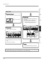
Simple method
To create chapters in a title, insert a chapter mark. Playback the content, locate a point where you want to divide, then
press the CHP DIVIDE button in the lid. You can insert a chapter mark also while recording, by pressing the CHP
DIVIDE button in the lid. (A chapter will also be placed in the recording when you pause.)
The point divides the chapter (into two). You can create multiple chapters by repeating the above operation.
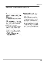
Notes
• Chapters cannot be created in the following modes:
Dubbing / Fast-reverse, Fast-forward / Slow-motion
• You cannot divide a title of a DVD-R/RW disc (Video mode) into chapters. It is possible to create chapters in a DVD-R/RW
disc (Video mode) in the following ways.
• By pressing the CHP DIVIDE button during recording at the desired points.
• By selecting an option that inserts chapter marks automatically during recording at regular intervals. (
page 28)
• Recording a programme onto the HDD to make chapter divisions on it, then dubbing the title to a DVD-R/RW (Video mode).
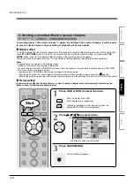
Precise method
If you want to modify the chapter division, or want to place a chapter mark more precisely monitoring the
frame counter, follow the procedures below.
1
Press HDD or DVD to select the drive.
HDD: Contents in the HDD
DVD: Contents in a loaded disc
(Contents recorded on other devices or those in a
finalized DVD-R/RW are not displayed.)
2
Press / / / to select a title.
• The titles in a folder can be edited.
3
Press QUICK MENU.
The Quick Menu appears.
ENTER
HDD
DVD-RAM
DVD-RW
(VR)
DVD-RW
(Video)
DVD-R
(VR)
DVD-VIDEO
VCD
CD
DVD-R
(Video)
HDD
DVD
TOP MENU
QUICK MENU
1
2
3
4
5
6
7
8
9
TV
DVD
INPUT SELECT
CHANNEL
MODE
RETURN
SLOW/REV
FWD/SLOW
PLAY
STOP
PAUSE
SKIP REV
SKIP FWD
–ADJUST
EXIT
QUICK MENU
OPERATION
INSTANT
SKIP
INSTANT
REPLAY
NUMBER
HDD
DVD
TOP MENU
MENU
MENU
TIMESLIP
CHANNEL
VOLUME
INPUT SELECT
OPEN/CLOSE
ENTER
Start
Cartoon
Sports
(0:00:00)
(1:25:30)
(0:00:00)
HDD (VR)
Title List
Page
CONTENT
MENU
2 / 5
LOCK
GARBAGE
Drama
Comedy
(1:25:30)
(0:00:00)
HDD :
01
03
04
02
e.g.
Содержание RD-XS24SB
Страница 10: ...Product Specification 2 4 MEMO ...
Страница 12: ...3 2 Software Update MEMO ...
Страница 19: ...Disassembly and Reaasembly 4 7 4 2 PCB Location Fig 4 7 PCB Location S M P S PCB JACK PCB MAIN PCB ...
Страница 20: ...4 8 Disassembly and Reaasembly MEMO ...
Страница 34: ...Troubleshooting 5 14 MEMO ...
Страница 35: ...6 1 6 Exploded View and Parts List 6 1 Cabinet Assembly Page 6 2 ...
Страница 38: ...Exploded Views and Parts List 6 4 MEMO ...
Страница 50: ...Electrical Parts List 7 12 MEMO ...
Страница 160: ...Operating Instructions 12 110 MEMO ...
Страница 173: ...1 1 SHIBAURA 1 CHOME MINATO KU TOKYO 105 8001 JAPAN ...
Страница 177: ...Block Diagrams 8 3 8 2 Digital Block Diagram ...
Страница 180: ...Block Diagrams 8 6 8 5 AIC01 MSP3417 Block Diagram ...
Страница 181: ...Block Diagrams 8 7 8 6 AIC02 AIC07 MC14052 Block Diagram ...
Страница 182: ...Block Diagrams 8 8 8 7 AIC03 AK5357 Block Diagram ...
Страница 183: ...Block Diagrams 8 9 8 8 AIC04 PCM1753 Block Diagram ...
Страница 184: ...Block Diagrams 8 10 8 9 KIC01 PT6961 Block Diagram ...
Страница 185: ...Block Diagrams 8 11 8 10 MIC01 78F4225 Block Diagram ...
Страница 187: ...Block Diagrams 8 13 8 12 SIC01 MM1647 Block Diagram ...
Страница 188: ...Block Diagrams 8 14 8 13 VIC01 74HC4051 Block Diagram ...
Страница 189: ...Block Diagrams 8 15 8 14 VIC05 MM1568 Block Diagram ...
Страница 190: ...Block Diagrams 8 16 MEMO ...
Страница 191: ...9 Wiring Diagram 9 1 ...
Страница 192: ...Wiring Diagram 9 2 MEMO ...
Страница 193: ...10 1 10 PCB Diagrams 10 1 S M P S PCB 10 2 Main PCB 10 3 Jack PCB 10 4 Key PCB 10 2 10 4 10 6 10 8 ...
Страница 194: ...PCB Diagrams 10 2 10 1 S M P S PCB COMPONENT SIDE ...
Страница 195: ...PCB Diagrams 10 3 CONDUCTOR SIDE ...
Страница 196: ...PCB Diagrams 10 4 10 2 Main PCB COMPONENT SIDE ...
Страница 198: ...PCB Diagrams 10 6 10 3 Jack PCB COMPONENT SIDE ...
Страница 199: ...PCB Diagrams 10 7 CONDUCTOR SIDE ...
Страница 200: ...PCB Diagrams 10 8 10 4 Key PCB COMPONENT SIDE CONDUCTOR SIDE ...
Страница 202: ...Schematic Diagrams 11 2 11 1 S M P S SMPS PCB ...
Страница 203: ...Schematic Diagrams 11 3 11 2 Main Main PCB ...
Страница 204: ...Schematic Diagrams 11 4 11 3 Audio Jack PCB ...
Страница 205: ...Schematic Diagrams 11 5 11 4 Video Jack PCB ...
Страница 206: ...Schematic Diagrams 11 6 11 5 AV switch Scart Jack PCB ...
Страница 207: ...Schematic Diagrams 11 7 11 6 Tuner Front in Connection Jack PCB ...
Страница 208: ...Schematic Diagrams 11 8 11 7 Micom Jack PCB ...
Страница 209: ...Schematic Diagrams 11 9 11 8 Key Key PCB ...
Страница 210: ...Schematic Diagrams 11 10 MEMO ...

