


Operating Instructions
12-55
Editing
Function
setup
Others
Introduction
Recording
Playback
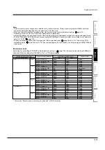
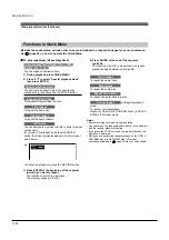
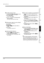
Using the time bar
The time bar shows the current progress in playback or recording.
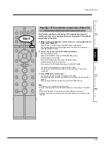
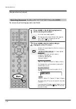
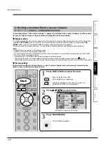
1
During playback or recording, press
QUICK MENU.
2
Press
/ to select “TimeBar”, then press
ENTER.
The time bar appears. (The actual display varies
depending on the disc.)
e.g. Playback
e.g. Recording
Locator (Shows the current location.)
Elapsed time
Total playing time of a current title
(In the case of a VIDEO CD or
audio CD, it shows the total
playing time of the disc.)
Elapsed recording time (per 30 minutes)
(Recording end time if it comes within 30
minutes.)
Elapsed time
QUICK MENU
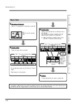
Changing the location of the time bar
While the time bar is displayed, press / .
The time bar shifts up and down.
Turning off the time bar
Press QUICK MENU and select “TimeBar” again,
then press ENTER.
Note
• Time display is an approximation.
01:30:00
00:00:00
00:30:00
00:00:00
00:55:00:00F
Location
00:18:00
Location
Chapter division
ENTER
Locator (Shows the current location.)
1
2
3
4
5
6
7
8
9
TV
DVD
INPUT SELECT
CHANNEL
MODE
RETURN
SLOW/REV
FWD/SLOW
PLAY
STOP
PAUSE
SKIP REV
SKIP FWD
–ADJUST
EXIT
QUICK MENU
OPERATION
INSTANT
SKIP
INSTANT
REPLAY
NUMBER
HDD
DVD
TOP MENU
MENU
MENU
TIMESLIP
CHANNEL
VOLUME
INPUT SELECT
OPEN/CLOSE
ENTER
Start
Содержание RD-XS24SB
Страница 10: ...Product Specification 2 4 MEMO ...
Страница 12: ...3 2 Software Update MEMO ...
Страница 19: ...Disassembly and Reaasembly 4 7 4 2 PCB Location Fig 4 7 PCB Location S M P S PCB JACK PCB MAIN PCB ...
Страница 20: ...4 8 Disassembly and Reaasembly MEMO ...
Страница 34: ...Troubleshooting 5 14 MEMO ...
Страница 35: ...6 1 6 Exploded View and Parts List 6 1 Cabinet Assembly Page 6 2 ...
Страница 38: ...Exploded Views and Parts List 6 4 MEMO ...
Страница 50: ...Electrical Parts List 7 12 MEMO ...
Страница 160: ...Operating Instructions 12 110 MEMO ...
Страница 173: ...1 1 SHIBAURA 1 CHOME MINATO KU TOKYO 105 8001 JAPAN ...
Страница 177: ...Block Diagrams 8 3 8 2 Digital Block Diagram ...
Страница 180: ...Block Diagrams 8 6 8 5 AIC01 MSP3417 Block Diagram ...
Страница 181: ...Block Diagrams 8 7 8 6 AIC02 AIC07 MC14052 Block Diagram ...
Страница 182: ...Block Diagrams 8 8 8 7 AIC03 AK5357 Block Diagram ...
Страница 183: ...Block Diagrams 8 9 8 8 AIC04 PCM1753 Block Diagram ...
Страница 184: ...Block Diagrams 8 10 8 9 KIC01 PT6961 Block Diagram ...
Страница 185: ...Block Diagrams 8 11 8 10 MIC01 78F4225 Block Diagram ...
Страница 187: ...Block Diagrams 8 13 8 12 SIC01 MM1647 Block Diagram ...
Страница 188: ...Block Diagrams 8 14 8 13 VIC01 74HC4051 Block Diagram ...
Страница 189: ...Block Diagrams 8 15 8 14 VIC05 MM1568 Block Diagram ...
Страница 190: ...Block Diagrams 8 16 MEMO ...
Страница 191: ...9 Wiring Diagram 9 1 ...
Страница 192: ...Wiring Diagram 9 2 MEMO ...
Страница 193: ...10 1 10 PCB Diagrams 10 1 S M P S PCB 10 2 Main PCB 10 3 Jack PCB 10 4 Key PCB 10 2 10 4 10 6 10 8 ...
Страница 194: ...PCB Diagrams 10 2 10 1 S M P S PCB COMPONENT SIDE ...
Страница 195: ...PCB Diagrams 10 3 CONDUCTOR SIDE ...
Страница 196: ...PCB Diagrams 10 4 10 2 Main PCB COMPONENT SIDE ...
Страница 198: ...PCB Diagrams 10 6 10 3 Jack PCB COMPONENT SIDE ...
Страница 199: ...PCB Diagrams 10 7 CONDUCTOR SIDE ...
Страница 200: ...PCB Diagrams 10 8 10 4 Key PCB COMPONENT SIDE CONDUCTOR SIDE ...
Страница 202: ...Schematic Diagrams 11 2 11 1 S M P S SMPS PCB ...
Страница 203: ...Schematic Diagrams 11 3 11 2 Main Main PCB ...
Страница 204: ...Schematic Diagrams 11 4 11 3 Audio Jack PCB ...
Страница 205: ...Schematic Diagrams 11 5 11 4 Video Jack PCB ...
Страница 206: ...Schematic Diagrams 11 6 11 5 AV switch Scart Jack PCB ...
Страница 207: ...Schematic Diagrams 11 7 11 6 Tuner Front in Connection Jack PCB ...
Страница 208: ...Schematic Diagrams 11 8 11 7 Micom Jack PCB ...
Страница 209: ...Schematic Diagrams 11 9 11 8 Key Key PCB ...
Страница 210: ...Schematic Diagrams 11 10 MEMO ...


