


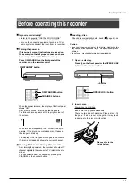


Is your recorder ready?
• Refer to the supplied “INSTALLATION GUIDE”
manual and finish the necessary preparations.
• Turn on the connected equipment such as a TV or
audio system and select the input from the recorder.
Turning the power on
(This owner’s manual instructions are based on
the assumption that all proper connections have
been completed and the TV is turned on.)
Press ON/STANDBY on the front panel of the
recorder or on the remote control.
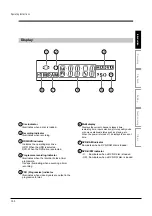
When the power turns on, the display of the front panel
shows “ON”.
After a few seconds, a start-up screen appears.
The following icon appears at the top right corner of
the screen.
When this icon disappears, the recorder is ready to
operate. If the disc drive contains a disc, it takes a
little longer to start up.
The display of the front panel changes to the counter.
If a disc is not loaded, it shows the current channel.
Viewing TV channels through this recorder
After turning the power on, the recorder will output TV
channel signals to the connected TV (also in the stop
mode).
You can select a desired channel by pressing the
CHANNEL or the number buttons.
Loading a disc
Check disc compatibility beforehand (
page 6) and
use a proper playable disc.
Caution
• Keep your fingers well clear of the disc tray. Neglecting this
may cause serious personal injury. Keep a close watch on
children.
• Do not use a cracked, deformed, or repaired disc.
1 Open the disc tray.
Press
on the front panel or the OPEN/CLOSE
button on the remote control.
2 Insert a disc.
Disc without a cartridge
Insert with the playback side down.
There are two kinds of disc size. Place a disc to fit
the guide. If a disc is out of the guide, it may result
in damage to the disc or malfunction.
Place a disc in the
inside hollow.
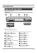
Before operating this recorder
ON/STANDBY button
TV
DVD
INPUT SELECT
CHANNEL
HDD
DVD
TOP MENU
MENU
MENU
TIMESLIP
CHANNEL
VOLUME
INPUT SELECT
OPEN/CLOSE
ON/STANDBY button
CHANNEL buttons
TV
DVD
INPUT SELECT
CHANNEL
HDD
DVD
TOP MENU
MENU
MENU
TIMESLIP
CHANNEL
VOLUME
INPUT SELECT
OPEN/CLOSE
button
OPEN/CLOSE button
Loading
e.g.
Operating Instructions
12-7
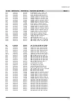
Содержание RD-XS24SB
Страница 10: ...Product Specification 2 4 MEMO ...
Страница 12: ...3 2 Software Update MEMO ...
Страница 19: ...Disassembly and Reaasembly 4 7 4 2 PCB Location Fig 4 7 PCB Location S M P S PCB JACK PCB MAIN PCB ...
Страница 20: ...4 8 Disassembly and Reaasembly MEMO ...
Страница 34: ...Troubleshooting 5 14 MEMO ...
Страница 35: ...6 1 6 Exploded View and Parts List 6 1 Cabinet Assembly Page 6 2 ...
Страница 38: ...Exploded Views and Parts List 6 4 MEMO ...
Страница 50: ...Electrical Parts List 7 12 MEMO ...
Страница 160: ...Operating Instructions 12 110 MEMO ...
Страница 173: ...1 1 SHIBAURA 1 CHOME MINATO KU TOKYO 105 8001 JAPAN ...
Страница 177: ...Block Diagrams 8 3 8 2 Digital Block Diagram ...
Страница 180: ...Block Diagrams 8 6 8 5 AIC01 MSP3417 Block Diagram ...
Страница 181: ...Block Diagrams 8 7 8 6 AIC02 AIC07 MC14052 Block Diagram ...
Страница 182: ...Block Diagrams 8 8 8 7 AIC03 AK5357 Block Diagram ...
Страница 183: ...Block Diagrams 8 9 8 8 AIC04 PCM1753 Block Diagram ...
Страница 184: ...Block Diagrams 8 10 8 9 KIC01 PT6961 Block Diagram ...
Страница 185: ...Block Diagrams 8 11 8 10 MIC01 78F4225 Block Diagram ...
Страница 187: ...Block Diagrams 8 13 8 12 SIC01 MM1647 Block Diagram ...
Страница 188: ...Block Diagrams 8 14 8 13 VIC01 74HC4051 Block Diagram ...
Страница 189: ...Block Diagrams 8 15 8 14 VIC05 MM1568 Block Diagram ...
Страница 190: ...Block Diagrams 8 16 MEMO ...
Страница 191: ...9 Wiring Diagram 9 1 ...
Страница 192: ...Wiring Diagram 9 2 MEMO ...
Страница 193: ...10 1 10 PCB Diagrams 10 1 S M P S PCB 10 2 Main PCB 10 3 Jack PCB 10 4 Key PCB 10 2 10 4 10 6 10 8 ...
Страница 194: ...PCB Diagrams 10 2 10 1 S M P S PCB COMPONENT SIDE ...
Страница 195: ...PCB Diagrams 10 3 CONDUCTOR SIDE ...
Страница 196: ...PCB Diagrams 10 4 10 2 Main PCB COMPONENT SIDE ...
Страница 198: ...PCB Diagrams 10 6 10 3 Jack PCB COMPONENT SIDE ...
Страница 199: ...PCB Diagrams 10 7 CONDUCTOR SIDE ...
Страница 200: ...PCB Diagrams 10 8 10 4 Key PCB COMPONENT SIDE CONDUCTOR SIDE ...
Страница 202: ...Schematic Diagrams 11 2 11 1 S M P S SMPS PCB ...
Страница 203: ...Schematic Diagrams 11 3 11 2 Main Main PCB ...
Страница 204: ...Schematic Diagrams 11 4 11 3 Audio Jack PCB ...
Страница 205: ...Schematic Diagrams 11 5 11 4 Video Jack PCB ...
Страница 206: ...Schematic Diagrams 11 6 11 5 AV switch Scart Jack PCB ...
Страница 207: ...Schematic Diagrams 11 7 11 6 Tuner Front in Connection Jack PCB ...
Страница 208: ...Schematic Diagrams 11 8 11 7 Micom Jack PCB ...
Страница 209: ...Schematic Diagrams 11 9 11 8 Key Key PCB ...
Страница 210: ...Schematic Diagrams 11 10 MEMO ...


