


Reference Information
14-3
14-2 DVD-Video Fromat
14-2-1 Main Features
1) Able to store up to 160 minutes of Movie by utilizing the MPEG-2 compression technology. ( Aver. 133min.)
2) Enables more than 500 lines of horizontal resolution. (Class corresponding to the Master Tapes used in
broadcasting stations)
3) Provides Dolby Digital 5.1ch Surround 3D sound, which enables theater quality sound (NTSC area).
•
For PAL areas, 1 of either MPEG-2 Audio or Dolby Digital must be selected.
4) Multi-Language
•
Able to store up to 8 languages of dubbing.
•
Able to store up to 32 subtitle languages.
5) Multi-Aspect Ratio
3TV Mode alternatives ; 16:9 Wide Screen (DVD Basic)/4:3 Pan & Scan/Letter Box.
6) Multi-Story
Possible to implement Interactive Viewing which enables the user to select the scenario.
7) Multi-Angle
Able to view the camera angle you selected among the scenes recorded with multiple camera angles.
Note
; The above media features must have the DVD Title that contains the appropriate contents to function
properly.
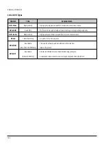
14-2-2 Audio & Video Specifications
Classification
DVD-Video Video-CD
LD
Compression
MPEG-2
MPEG-1
Analog
Pixel
720 x 480
352 x 240
VIDEO
Horizontal resolution
Max. 500 Lines
Max. 250 Lines
Max.420 Lines
Compression rate
1/40
1/140
Analog
Transmission speed
Max. 9.8Mbps (variable)
1.15Mbps (fixed)
TV aspect
16:9 / 4:3
4:3
4:3
Audio
Max. 8 streams
2CH stereo
Recording type
Dolby Digital
Linear PCM
MPEG-1 Layer 2
AUDIO
Transmission rate
448Kbps/stream
6.144Mbps/stream
224Kbps
or
Channel
5.1CH/stream
8CH/stream
2CH
Sampling frequency
48KHz
16, 20, 24Bit/48, 96KHz
16Bit/44.1KHz
2 Analog CH.
2 Digital CH.
(16Bit/44.1KHz)
1 Analog CH.
1 Stream of Dolby Digital
2 Digital CH.
(16Bit/44.1KHz)
Содержание RD-XS24SB
Страница 10: ...Product Specification 2 4 MEMO ...
Страница 12: ...3 2 Software Update MEMO ...
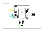
Страница 19: ...Disassembly and Reaasembly 4 7 4 2 PCB Location Fig 4 7 PCB Location S M P S PCB JACK PCB MAIN PCB ...
Страница 20: ...4 8 Disassembly and Reaasembly MEMO ...
Страница 34: ...Troubleshooting 5 14 MEMO ...
Страница 35: ...6 1 6 Exploded View and Parts List 6 1 Cabinet Assembly Page 6 2 ...
Страница 38: ...Exploded Views and Parts List 6 4 MEMO ...
Страница 50: ...Electrical Parts List 7 12 MEMO ...
Страница 160: ...Operating Instructions 12 110 MEMO ...
Страница 173: ...1 1 SHIBAURA 1 CHOME MINATO KU TOKYO 105 8001 JAPAN ...
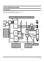
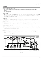
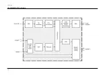
Страница 177: ...Block Diagrams 8 3 8 2 Digital Block Diagram ...
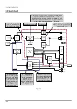
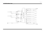
Страница 180: ...Block Diagrams 8 6 8 5 AIC01 MSP3417 Block Diagram ...
Страница 181: ...Block Diagrams 8 7 8 6 AIC02 AIC07 MC14052 Block Diagram ...
Страница 182: ...Block Diagrams 8 8 8 7 AIC03 AK5357 Block Diagram ...
Страница 183: ...Block Diagrams 8 9 8 8 AIC04 PCM1753 Block Diagram ...
Страница 184: ...Block Diagrams 8 10 8 9 KIC01 PT6961 Block Diagram ...
Страница 185: ...Block Diagrams 8 11 8 10 MIC01 78F4225 Block Diagram ...
Страница 187: ...Block Diagrams 8 13 8 12 SIC01 MM1647 Block Diagram ...
Страница 188: ...Block Diagrams 8 14 8 13 VIC01 74HC4051 Block Diagram ...
Страница 189: ...Block Diagrams 8 15 8 14 VIC05 MM1568 Block Diagram ...
Страница 190: ...Block Diagrams 8 16 MEMO ...
Страница 191: ...9 Wiring Diagram 9 1 ...
Страница 192: ...Wiring Diagram 9 2 MEMO ...
Страница 193: ...10 1 10 PCB Diagrams 10 1 S M P S PCB 10 2 Main PCB 10 3 Jack PCB 10 4 Key PCB 10 2 10 4 10 6 10 8 ...
Страница 194: ...PCB Diagrams 10 2 10 1 S M P S PCB COMPONENT SIDE ...
Страница 195: ...PCB Diagrams 10 3 CONDUCTOR SIDE ...
Страница 196: ...PCB Diagrams 10 4 10 2 Main PCB COMPONENT SIDE ...
Страница 198: ...PCB Diagrams 10 6 10 3 Jack PCB COMPONENT SIDE ...
Страница 199: ...PCB Diagrams 10 7 CONDUCTOR SIDE ...
Страница 200: ...PCB Diagrams 10 8 10 4 Key PCB COMPONENT SIDE CONDUCTOR SIDE ...
Страница 202: ...Schematic Diagrams 11 2 11 1 S M P S SMPS PCB ...
Страница 203: ...Schematic Diagrams 11 3 11 2 Main Main PCB ...
Страница 204: ...Schematic Diagrams 11 4 11 3 Audio Jack PCB ...
Страница 205: ...Schematic Diagrams 11 5 11 4 Video Jack PCB ...
Страница 206: ...Schematic Diagrams 11 6 11 5 AV switch Scart Jack PCB ...
Страница 207: ...Schematic Diagrams 11 7 11 6 Tuner Front in Connection Jack PCB ...
Страница 208: ...Schematic Diagrams 11 8 11 7 Micom Jack PCB ...
Страница 209: ...Schematic Diagrams 11 9 11 8 Key Key PCB ...
Страница 210: ...Schematic Diagrams 11 10 MEMO ...


