Programming a recording (REC MENU) (Continued)
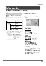
Deleting a timer program
The maximum timer program capacity is 32. Any new
program will be rejected if the recorder is full. To enter a
new program, you must cancel an existing one.
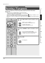
1) Press MENU.
2) Press / to select “Timer recording”, then
press ENTER.
3) Press
/ to select a timer program you want
to delete.
4) Press QUICK MENU.
The Quick Menu appears.
5) Press / to select “Program cancel”, then
press ENTER.
Check the message, then delete the entry.
Note
• You cannot delete a timer program while another is
executed.
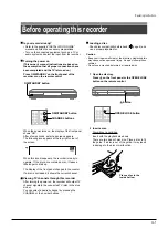
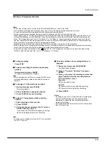
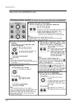
To stop a programmed recording
1) Select the recording drive by pressing HDD or
DVD twice.
2) Press on the front panel twice.
When you press the button once, a message
appears. While the message is displayed, press the
button once again.
Note
• If you press the STOP button on the remote control, a
message appears. Select “Yes”, then press the ENTER
button.
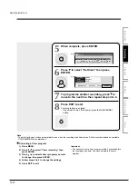
Checking the remaining volume
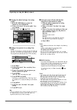
1) On REC MENU Timer Programming, press
QUICK MENU.
2) Press / to select “Disc budget calculation”
then press ENTER.
The Disc budget calculation menu appears.
3) Press / to select a timer program, then
press ENTER.
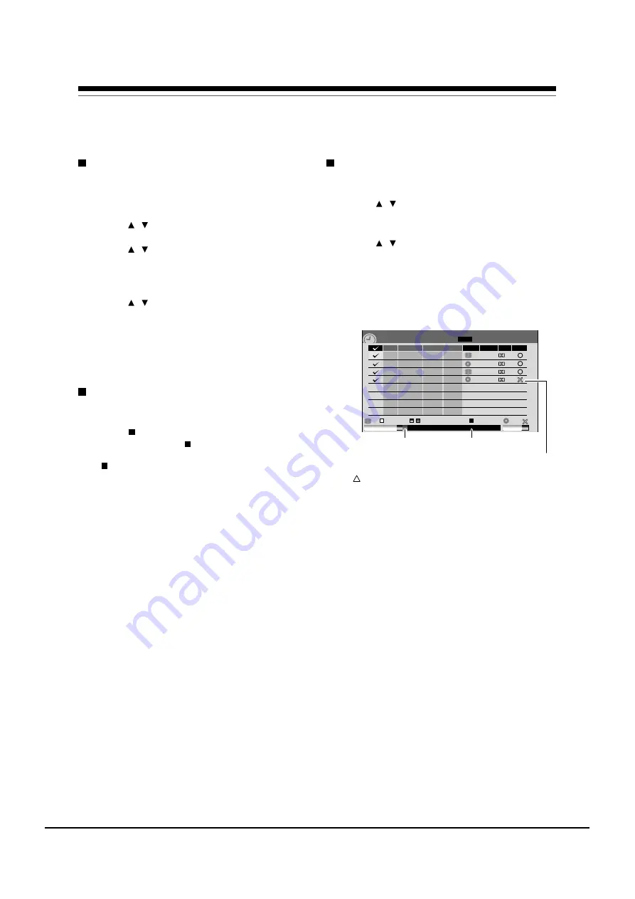
The recorder calculates on a bar graph how much
a specific program (identified by a check mark) will
occupy on the disc.
Pressing the ADJUST button can display or remove
the check mark.
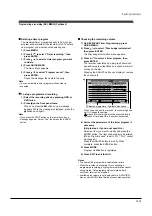
4) Correct the parameters of the timer program if
necessary.
(Skip to step 6 if you do not need this.)
Select an item you want to modify and press the
ENTER button. The item will be ready to be altered.
(When “High rate save” is set to “On”, “Pict.” cannot
be changed.)
Press the ADJUST button to modify. When
complete, press the ENTER button.
5) Press MODE.
Program modification is registered.
6) Press EXIT to exit the GUI.
Notes
• The nearest 48 programs are calculated at a time.
• While the recorder is preparing for or executing a
programmed recording, any program modification cannot
be registered. Only programs which will start after 5
minutes or later can be modified.
• Available disc volume is not displayed for a DVD-R/RW
disc on which DVD-Video finalize process was executed.
e.g.
10/23(Su)17:50
Disc budget calculation
REC
MENU
Ch
Date
Start
End
Pict. Audio
Page
1 / 1
1
10
42
4
-
10/30(Su)
11/16(We)
11/19(Sa)
11/26(Sa)
7:00
8:30
-
9:30
10:00
-
10:30
11:30
-
8:30
11:30
MN 6.6
HDD
HDD
HDD
D/M2
MN 6.6
D/M2
LP 2.2
D/M1
SP 4.6
D/M2
DVD
DVD
DVD
Media
Result
Elapsed
Available
Selected(current)
(
)
Selected programme Available disc space
When the entry item is marked X, the recording does
not fit. Change the setting.
means this recording will not be executed due to
limitation of recording time, if another is executed.
Operating Instructions
12-19
Содержание RD-XS24SB
Страница 10: ...Product Specification 2 4 MEMO ...
Страница 12: ...3 2 Software Update MEMO ...
Страница 19: ...Disassembly and Reaasembly 4 7 4 2 PCB Location Fig 4 7 PCB Location S M P S PCB JACK PCB MAIN PCB ...
Страница 20: ...4 8 Disassembly and Reaasembly MEMO ...
Страница 34: ...Troubleshooting 5 14 MEMO ...
Страница 35: ...6 1 6 Exploded View and Parts List 6 1 Cabinet Assembly Page 6 2 ...
Страница 38: ...Exploded Views and Parts List 6 4 MEMO ...
Страница 50: ...Electrical Parts List 7 12 MEMO ...
Страница 160: ...Operating Instructions 12 110 MEMO ...
Страница 173: ...1 1 SHIBAURA 1 CHOME MINATO KU TOKYO 105 8001 JAPAN ...
Страница 177: ...Block Diagrams 8 3 8 2 Digital Block Diagram ...
Страница 180: ...Block Diagrams 8 6 8 5 AIC01 MSP3417 Block Diagram ...
Страница 181: ...Block Diagrams 8 7 8 6 AIC02 AIC07 MC14052 Block Diagram ...
Страница 182: ...Block Diagrams 8 8 8 7 AIC03 AK5357 Block Diagram ...
Страница 183: ...Block Diagrams 8 9 8 8 AIC04 PCM1753 Block Diagram ...
Страница 184: ...Block Diagrams 8 10 8 9 KIC01 PT6961 Block Diagram ...
Страница 185: ...Block Diagrams 8 11 8 10 MIC01 78F4225 Block Diagram ...
Страница 187: ...Block Diagrams 8 13 8 12 SIC01 MM1647 Block Diagram ...
Страница 188: ...Block Diagrams 8 14 8 13 VIC01 74HC4051 Block Diagram ...
Страница 189: ...Block Diagrams 8 15 8 14 VIC05 MM1568 Block Diagram ...
Страница 190: ...Block Diagrams 8 16 MEMO ...
Страница 191: ...9 Wiring Diagram 9 1 ...
Страница 192: ...Wiring Diagram 9 2 MEMO ...
Страница 193: ...10 1 10 PCB Diagrams 10 1 S M P S PCB 10 2 Main PCB 10 3 Jack PCB 10 4 Key PCB 10 2 10 4 10 6 10 8 ...
Страница 194: ...PCB Diagrams 10 2 10 1 S M P S PCB COMPONENT SIDE ...
Страница 195: ...PCB Diagrams 10 3 CONDUCTOR SIDE ...
Страница 196: ...PCB Diagrams 10 4 10 2 Main PCB COMPONENT SIDE ...
Страница 198: ...PCB Diagrams 10 6 10 3 Jack PCB COMPONENT SIDE ...
Страница 199: ...PCB Diagrams 10 7 CONDUCTOR SIDE ...
Страница 200: ...PCB Diagrams 10 8 10 4 Key PCB COMPONENT SIDE CONDUCTOR SIDE ...
Страница 202: ...Schematic Diagrams 11 2 11 1 S M P S SMPS PCB ...
Страница 203: ...Schematic Diagrams 11 3 11 2 Main Main PCB ...
Страница 204: ...Schematic Diagrams 11 4 11 3 Audio Jack PCB ...
Страница 205: ...Schematic Diagrams 11 5 11 4 Video Jack PCB ...
Страница 206: ...Schematic Diagrams 11 6 11 5 AV switch Scart Jack PCB ...
Страница 207: ...Schematic Diagrams 11 7 11 6 Tuner Front in Connection Jack PCB ...
Страница 208: ...Schematic Diagrams 11 8 11 7 Micom Jack PCB ...
Страница 209: ...Schematic Diagrams 11 9 11 8 Key Key PCB ...
Страница 210: ...Schematic Diagrams 11 10 MEMO ...


