
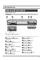
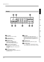

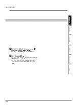


Playback
Recording
Editing
Others
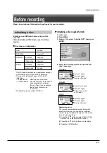
Introduction
Function
setup
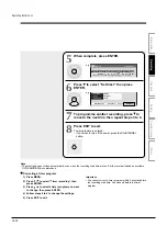
Naming a disc
(1) Press the / buttons to select “Edit” of “Disc
Name” then press the ENTER button.
(2) Enter a disc name following the procedure of
“Entering Characters” (
page 128).
(3) Press the MODE button to save the name then
exit.
Selecting the DVD mode
(1) Press the / buttons to select “Edit” of “DVD
mode” then press the ENTER button.
(2) Press the / buttons to select the mode.
(3) Press the ENTER button.
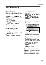
5) Press / / / to select “Start”, then press
ENTER.
6) Read the message, and press / to select
“Start”, then press ENTER.
Initializing starts.
Notes
• Discs may be unusable if there are deterioration or defects
in it.
• When a finalized DVD-RW is loaded, playback starts
automatically. To initialize, stop the playback then follow
the above procedure.
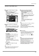
Initializing a disc (Physical format)
Use this method when a DVD-RAM is not recovered by
logical format method or when the recorder does not
read a DVD-RAM which has been used. (There is no
guarantee that all such discs will be recovered.)
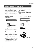
1) Load a DVD-RAM.
2) Open the lid of the remote control, and press
SETUP.
(Alternatively, press MENU and select “Other
settings” and press ENTER.)
3) Press RETURN then / to select
“Management settings”, and press ENTER.
4) Press / to select “DVD-RAM physical
format” then press ENTER.
5) Read the message, and press / to select
“Yes”, then press ENTER.
6) Ask the question on shutting down using / ,
then press ENTER.
Notes
• The physical format process may fail if executed to a dirty
DVD-RAM. Also the disc may be difficult to record even it is
finished. Before executing DVD-RAM physical format
process, be sure to confirm the disc is not dirty. Clean it if
necessary. If the disc has scratches or dust beyond
cleaner’s efficacy, do not execute DVD-RAM physical
format process on the disc.
• The following DVD-RAM require physical formatting:
– A disc which is not formatted correctly.
– The disc which has some errors during writing because
of dirt on the disc, and cannot be further recorded, or
cannot initialize normally.
• Physical formatting does not work if the disc contains a lot
of voids beyond the limitation of the recorder.
• If an error occurs in physical formatting, “ERR01” appears
in the front panel display. To turn it off, press the DISPLAY
button.
DV D format
Start
Cancel
Entire disc contents will be
erased if disc is formatted.
Proceed?
Yes
No
Warning: It will take approximately
70 minutes to format a 4.7GB DVD
and all data will be erased.
Confirm that timer programming is
not scheduled. Proceed?
Operating Instructions
12-14
Содержание RD-XS24SB
Страница 10: ...Product Specification 2 4 MEMO ...
Страница 12: ...3 2 Software Update MEMO ...
Страница 19: ...Disassembly and Reaasembly 4 7 4 2 PCB Location Fig 4 7 PCB Location S M P S PCB JACK PCB MAIN PCB ...
Страница 20: ...4 8 Disassembly and Reaasembly MEMO ...
Страница 34: ...Troubleshooting 5 14 MEMO ...
Страница 35: ...6 1 6 Exploded View and Parts List 6 1 Cabinet Assembly Page 6 2 ...
Страница 38: ...Exploded Views and Parts List 6 4 MEMO ...
Страница 50: ...Electrical Parts List 7 12 MEMO ...
Страница 160: ...Operating Instructions 12 110 MEMO ...
Страница 173: ...1 1 SHIBAURA 1 CHOME MINATO KU TOKYO 105 8001 JAPAN ...
Страница 177: ...Block Diagrams 8 3 8 2 Digital Block Diagram ...
Страница 180: ...Block Diagrams 8 6 8 5 AIC01 MSP3417 Block Diagram ...
Страница 181: ...Block Diagrams 8 7 8 6 AIC02 AIC07 MC14052 Block Diagram ...
Страница 182: ...Block Diagrams 8 8 8 7 AIC03 AK5357 Block Diagram ...
Страница 183: ...Block Diagrams 8 9 8 8 AIC04 PCM1753 Block Diagram ...
Страница 184: ...Block Diagrams 8 10 8 9 KIC01 PT6961 Block Diagram ...
Страница 185: ...Block Diagrams 8 11 8 10 MIC01 78F4225 Block Diagram ...
Страница 187: ...Block Diagrams 8 13 8 12 SIC01 MM1647 Block Diagram ...
Страница 188: ...Block Diagrams 8 14 8 13 VIC01 74HC4051 Block Diagram ...
Страница 189: ...Block Diagrams 8 15 8 14 VIC05 MM1568 Block Diagram ...
Страница 190: ...Block Diagrams 8 16 MEMO ...
Страница 191: ...9 Wiring Diagram 9 1 ...
Страница 192: ...Wiring Diagram 9 2 MEMO ...
Страница 193: ...10 1 10 PCB Diagrams 10 1 S M P S PCB 10 2 Main PCB 10 3 Jack PCB 10 4 Key PCB 10 2 10 4 10 6 10 8 ...
Страница 194: ...PCB Diagrams 10 2 10 1 S M P S PCB COMPONENT SIDE ...
Страница 195: ...PCB Diagrams 10 3 CONDUCTOR SIDE ...
Страница 196: ...PCB Diagrams 10 4 10 2 Main PCB COMPONENT SIDE ...
Страница 198: ...PCB Diagrams 10 6 10 3 Jack PCB COMPONENT SIDE ...
Страница 199: ...PCB Diagrams 10 7 CONDUCTOR SIDE ...
Страница 200: ...PCB Diagrams 10 8 10 4 Key PCB COMPONENT SIDE CONDUCTOR SIDE ...
Страница 202: ...Schematic Diagrams 11 2 11 1 S M P S SMPS PCB ...
Страница 203: ...Schematic Diagrams 11 3 11 2 Main Main PCB ...
Страница 204: ...Schematic Diagrams 11 4 11 3 Audio Jack PCB ...
Страница 205: ...Schematic Diagrams 11 5 11 4 Video Jack PCB ...
Страница 206: ...Schematic Diagrams 11 6 11 5 AV switch Scart Jack PCB ...
Страница 207: ...Schematic Diagrams 11 7 11 6 Tuner Front in Connection Jack PCB ...
Страница 208: ...Schematic Diagrams 11 8 11 7 Micom Jack PCB ...
Страница 209: ...Schematic Diagrams 11 9 11 8 Key Key PCB ...
Страница 210: ...Schematic Diagrams 11 10 MEMO ...


