


Operating Instructions
12-98
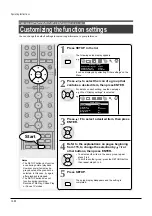
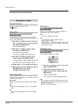
Customizing the function settings
You can change the default settings to customize performance to your preference.
Notes
• The SETUP button can function
even during normal playback.
However some items may be
grayed out and they cannot be
selected. In this case, try again
after playback is stopped.
• The SETUP button does not
function during recording,
Recorded Title Play, Chase Play
or Pause TV modes.
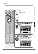
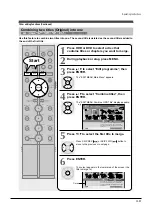
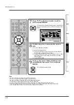
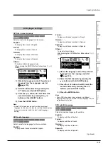
1
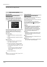
Press SETUP in the lid.
The following setup display appears.
It can be displayed by selecting “Other settings” on the
Menu.
2
Press / to select the icon of a group that
contains a desired item, then press ENTER.
For details on each setting, see the next page.
e.g. When “Display settings” is selected:
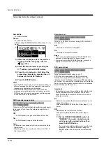
3
Press / to select a desired item, then press
ENTER.
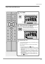
4
Refer to the explanations on pages beginning
from 115, to change the selection by / or
other buttons, then press ENTER.
• To select another item in the same group, repeat
steps 3 to 4.
• To shift to another group, press the RETURN button
then repeat steps 2 to 4.
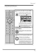
5
Press SETUP.
The setup display disappears and the setting is
completed.
1
2
3
4
5
6
7
8
9
+10
0
CHANNEL
MODE
RETURN
SLOW/REV
FWD/SLOW
PLAY
STOP
PAUSE
REC
SKIP REV
SKIP FWD
–ADJUST
TV/DVR
DELETE
CLEAR
EXIT
ENTER
QUICK MENU
OPERATION
INSTANT
SKIP
INSTANT
REPLAY
NUMBER
HDD
DVD
TOP MENU
MENU
MENU
TIMESLIP
CHANNEL
VOLUME
INPUT SELECT
CHP DIVIDE ANGLE
SUBTITLE
AUDIO
REC MODE ZOOM
SEARCH DISPLAY
PROGRESSIVE EXTEND
SETUP
REMAIN
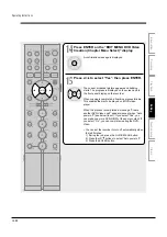
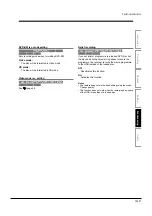
e.g.
DVD subtitle language
DVD d
i
l
DVD audio language
DVD player settings
DVD disc menu language
English
English
No subtitle
O
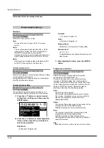
e.g.
Transparency
Startup screen
On screen display
Display settings
Background
Screen protector
TV shape
4:3LB
On
25%
On Animation
On
Blue
SETUP
ENTER
ENTER
ENTER
SETUP
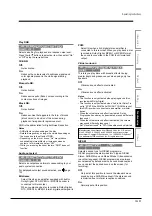
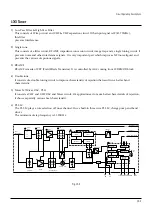
HDD
DVD-RAM
DVD-RW
(VR)
DVD-RW
(Video)
DVD-R
(VR)
DVD-VIDEO
VCD
CD
DVD-R
(Video)
Start
Содержание RD-XS24SB
Страница 10: ...Product Specification 2 4 MEMO ...
Страница 12: ...3 2 Software Update MEMO ...
Страница 19: ...Disassembly and Reaasembly 4 7 4 2 PCB Location Fig 4 7 PCB Location S M P S PCB JACK PCB MAIN PCB ...
Страница 20: ...4 8 Disassembly and Reaasembly MEMO ...
Страница 34: ...Troubleshooting 5 14 MEMO ...
Страница 35: ...6 1 6 Exploded View and Parts List 6 1 Cabinet Assembly Page 6 2 ...
Страница 38: ...Exploded Views and Parts List 6 4 MEMO ...
Страница 50: ...Electrical Parts List 7 12 MEMO ...
Страница 160: ...Operating Instructions 12 110 MEMO ...
Страница 173: ...1 1 SHIBAURA 1 CHOME MINATO KU TOKYO 105 8001 JAPAN ...
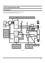
Страница 177: ...Block Diagrams 8 3 8 2 Digital Block Diagram ...
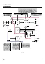
Страница 180: ...Block Diagrams 8 6 8 5 AIC01 MSP3417 Block Diagram ...
Страница 181: ...Block Diagrams 8 7 8 6 AIC02 AIC07 MC14052 Block Diagram ...
Страница 182: ...Block Diagrams 8 8 8 7 AIC03 AK5357 Block Diagram ...
Страница 183: ...Block Diagrams 8 9 8 8 AIC04 PCM1753 Block Diagram ...
Страница 184: ...Block Diagrams 8 10 8 9 KIC01 PT6961 Block Diagram ...
Страница 185: ...Block Diagrams 8 11 8 10 MIC01 78F4225 Block Diagram ...
Страница 187: ...Block Diagrams 8 13 8 12 SIC01 MM1647 Block Diagram ...
Страница 188: ...Block Diagrams 8 14 8 13 VIC01 74HC4051 Block Diagram ...
Страница 189: ...Block Diagrams 8 15 8 14 VIC05 MM1568 Block Diagram ...
Страница 190: ...Block Diagrams 8 16 MEMO ...
Страница 191: ...9 Wiring Diagram 9 1 ...
Страница 192: ...Wiring Diagram 9 2 MEMO ...
Страница 193: ...10 1 10 PCB Diagrams 10 1 S M P S PCB 10 2 Main PCB 10 3 Jack PCB 10 4 Key PCB 10 2 10 4 10 6 10 8 ...
Страница 194: ...PCB Diagrams 10 2 10 1 S M P S PCB COMPONENT SIDE ...
Страница 195: ...PCB Diagrams 10 3 CONDUCTOR SIDE ...
Страница 196: ...PCB Diagrams 10 4 10 2 Main PCB COMPONENT SIDE ...
Страница 198: ...PCB Diagrams 10 6 10 3 Jack PCB COMPONENT SIDE ...
Страница 199: ...PCB Diagrams 10 7 CONDUCTOR SIDE ...
Страница 200: ...PCB Diagrams 10 8 10 4 Key PCB COMPONENT SIDE CONDUCTOR SIDE ...
Страница 202: ...Schematic Diagrams 11 2 11 1 S M P S SMPS PCB ...
Страница 203: ...Schematic Diagrams 11 3 11 2 Main Main PCB ...
Страница 204: ...Schematic Diagrams 11 4 11 3 Audio Jack PCB ...
Страница 205: ...Schematic Diagrams 11 5 11 4 Video Jack PCB ...
Страница 206: ...Schematic Diagrams 11 6 11 5 AV switch Scart Jack PCB ...
Страница 207: ...Schematic Diagrams 11 7 11 6 Tuner Front in Connection Jack PCB ...
Страница 208: ...Schematic Diagrams 11 8 11 7 Micom Jack PCB ...
Страница 209: ...Schematic Diagrams 11 9 11 8 Key Key PCB ...
Страница 210: ...Schematic Diagrams 11 10 MEMO ...


