


Operating Instructions
12-92
Editing
Function
setup
Others
Introduction
Recording
Playback
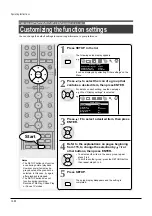
2
PLAY
8
PAUSE
ENTER
HDD (VR)
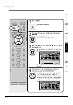
CONTENT
MENU
00:29:50
2005/10/12 23:00 Ch:6
00:00:00
(0:29:50)
00:06:25:23F
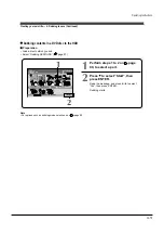
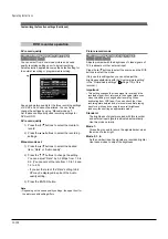
Location
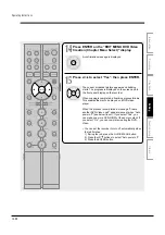
Create thumbnail
Select desired thumbnail image via
remote. To set, press enter.
Title:002
Chapter:0001
e.g.
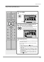
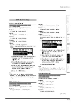
HDD (VR)
CONTENT
MENU
HDD :
Title List
Page
4 / 5
(0:53:45)
(0:29:50)
Play List
(0:54:30)
(0:51:28)
(0:52:40)
(0:30:08)
Summer day
Singing birds
Cruise
Cat show
Fishing lesson
Country life
e.g.
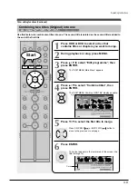
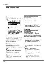
4
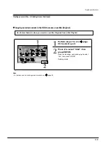
Press PLAY to start playback.
Locate a scene you want to capture as a thumbnail.
You can use the following buttons.
SLOW/REV, FWD/SLOW, SKIP REV, SKIP FWD,
PAUSE, ADJUST, etc.
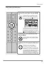
5
At the point where you want to capture a
thumbnail image, press PAUSE.
6
Press ENTER.
The “CONTENT MENU” returns. The selected scene is
displayed as a thumbnail.
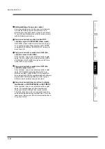
Notes
• There may be a small difference between a thumbnail made on the “Create thumbnail” display and that displayed in the
“CONTENT MENU”. Operation with the SLOW/REV or FWD/SLOW buttons may extend the difference.
• You cannot create thumbnails of chapters in a title that contains a still picture.
• If you create a chapter thumbnail, and then record or edit the disc on other devices, the chapter thumbnail may return to
the top of the chapter.
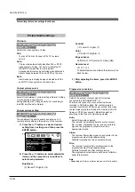
1
2
3
4
5
6
7
8
9
+10
0
TV
DVD
INPUT SELECT
CHANNEL
MODE
RETURN
SLOW/REV
FWD/SLOW
PLAY
STOP
PAUSE
REC
SKIP REV
SKIP FWD
–ADJUST
TV/DVR
DELETE
CLEAR
EXIT
QUICK MENU
OPERATION
INSTANT
SKIP
INSTANT
REPLAY
NUMBER
HDD
DVD
TOP MENU
MENU
MENU
TIMESLIP
CHANNEL
VOLUME
INPUT SELECT
OPEN/CLOSE
CHP DIVIDE ANGLE
SUBTITLE
AUDIO
REC MODE ZOOM
SEARCH DISPLAY
PROGRESSIVE EXTEND
SETUP
REMAIN
ENTER
Содержание RD-XS24SB
Страница 10: ...Product Specification 2 4 MEMO ...
Страница 12: ...3 2 Software Update MEMO ...
Страница 19: ...Disassembly and Reaasembly 4 7 4 2 PCB Location Fig 4 7 PCB Location S M P S PCB JACK PCB MAIN PCB ...
Страница 20: ...4 8 Disassembly and Reaasembly MEMO ...
Страница 34: ...Troubleshooting 5 14 MEMO ...
Страница 35: ...6 1 6 Exploded View and Parts List 6 1 Cabinet Assembly Page 6 2 ...
Страница 38: ...Exploded Views and Parts List 6 4 MEMO ...
Страница 50: ...Electrical Parts List 7 12 MEMO ...
Страница 160: ...Operating Instructions 12 110 MEMO ...
Страница 173: ...1 1 SHIBAURA 1 CHOME MINATO KU TOKYO 105 8001 JAPAN ...
Страница 177: ...Block Diagrams 8 3 8 2 Digital Block Diagram ...
Страница 180: ...Block Diagrams 8 6 8 5 AIC01 MSP3417 Block Diagram ...
Страница 181: ...Block Diagrams 8 7 8 6 AIC02 AIC07 MC14052 Block Diagram ...
Страница 182: ...Block Diagrams 8 8 8 7 AIC03 AK5357 Block Diagram ...
Страница 183: ...Block Diagrams 8 9 8 8 AIC04 PCM1753 Block Diagram ...
Страница 184: ...Block Diagrams 8 10 8 9 KIC01 PT6961 Block Diagram ...
Страница 185: ...Block Diagrams 8 11 8 10 MIC01 78F4225 Block Diagram ...
Страница 187: ...Block Diagrams 8 13 8 12 SIC01 MM1647 Block Diagram ...
Страница 188: ...Block Diagrams 8 14 8 13 VIC01 74HC4051 Block Diagram ...
Страница 189: ...Block Diagrams 8 15 8 14 VIC05 MM1568 Block Diagram ...
Страница 190: ...Block Diagrams 8 16 MEMO ...
Страница 191: ...9 Wiring Diagram 9 1 ...
Страница 192: ...Wiring Diagram 9 2 MEMO ...
Страница 193: ...10 1 10 PCB Diagrams 10 1 S M P S PCB 10 2 Main PCB 10 3 Jack PCB 10 4 Key PCB 10 2 10 4 10 6 10 8 ...
Страница 194: ...PCB Diagrams 10 2 10 1 S M P S PCB COMPONENT SIDE ...
Страница 195: ...PCB Diagrams 10 3 CONDUCTOR SIDE ...
Страница 196: ...PCB Diagrams 10 4 10 2 Main PCB COMPONENT SIDE ...
Страница 198: ...PCB Diagrams 10 6 10 3 Jack PCB COMPONENT SIDE ...
Страница 199: ...PCB Diagrams 10 7 CONDUCTOR SIDE ...
Страница 200: ...PCB Diagrams 10 8 10 4 Key PCB COMPONENT SIDE CONDUCTOR SIDE ...
Страница 202: ...Schematic Diagrams 11 2 11 1 S M P S SMPS PCB ...
Страница 203: ...Schematic Diagrams 11 3 11 2 Main Main PCB ...
Страница 204: ...Schematic Diagrams 11 4 11 3 Audio Jack PCB ...
Страница 205: ...Schematic Diagrams 11 5 11 4 Video Jack PCB ...
Страница 206: ...Schematic Diagrams 11 6 11 5 AV switch Scart Jack PCB ...
Страница 207: ...Schematic Diagrams 11 7 11 6 Tuner Front in Connection Jack PCB ...
Страница 208: ...Schematic Diagrams 11 8 11 7 Micom Jack PCB ...
Страница 209: ...Schematic Diagrams 11 9 11 8 Key Key PCB ...
Страница 210: ...Schematic Diagrams 11 10 MEMO ...


