Hardware Principle 4-9
4.2.7
Display
LVDS
3.3V
Display
High-voltage
LCD
screen
Parameter
board
I2C
3.3V
Inverter board
ON/OFF
12V
Brightness
control
Main board
IO board
12V
3.3V
Multifunction FPGA
LVDS
I2C
triode
triode
Control signal
of switch
Brightness
PWM
ON/
OFF
Brightness
control
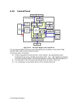
Figure 4-9 Principle Diagram of Display
Monitor mainly consists of the inverter board, LCD and the parameter board.
Function describes as following:
The inverter board produces high voltage to illuminate backlight of LCD which is adjusted
by signal control switch and brightness of the IO board output.
Color temperature and Gamma correction data memory in parameter board used matches
LCD so that the corresponding display effect shall be consistent.
Multifunction FPGA generates switch control signal which drives triode to control inverter to
open or shut off high-voltage output.
Multifunctional FPGA generates PWM signal, which drives triode to control output
high-voltage of the inverter to adjust the brightness of the display.
Multifunctional FPGA outputs LVDS digital signal of display, which is sent to screen directly.
Multifunctional FPGA communicates with parameter via 12C signal and supports to adjust
parameters of display.
Содержание Z6
Страница 2: ......
Страница 14: ......
Страница 16: ...2 2 Product Specifications Left side 9 4 7 5 6 8 ...
Страница 72: ......
Страница 119: ...Structure and Assembly Disassembly 7 35 图 7 59 Disassembly of Speaker 8 ...
Страница 120: ......
Страница 132: ......
Страница 142: ......
Страница 152: ......
Страница 168: ......
Страница 171: ...Phantom Usage Illustration B 3 ...
Страница 172: ......
Страница 173: ...P N 046 010452 00 5 0 ...


