EXTERNAL BUS
14-19
14
14.2.3.5
Recovery States
The state following the last data transfer of an access is a recovery (Tr) state. By default, i960 Jx
microprocessor bus transactions have one recovery state. External logic can cause additional
recovery states to be inserted by driving the RDYRCV pin low at the end of Tr.
Recovery wait states are an important feature for the Jx because it employs a multiplexed bus.
Slow memory and I/O devices often need a long time to turn off their output drivers on read
accesses before the microprocessor drives the address for the next bus access. Recovery wait states
are also useful to force a delay between back-to-back accesses to I/O devices with their own
specific access recovery requirements.
System ready logic is often described as normally-ready or normally-not-ready. Normally-ready
logic asserts a microprocessor’s input pin during all bus states, except when wait states are desired.
Normally-not-ready logic deasserts a processor’s input pin during all bus states, except when the
processor is ready. The subtle nomenclature distinction is important for i960 Jx microprocessor
systems because the active sense of the RDYRCV pin reverses for recovery states. During the Tr
state, logic 0 means “continue to recover” or “not ready”; for Tw/Td states, logic 0 means “ready”.
Logic must assure “ready” and “not recover” are generated to terminate an access properly. Be
certain to not hang the processor with endless recovery states. Conventional ready logic implemented
as normally-not-ready will operate correctly (but without adding turnaround wait states).
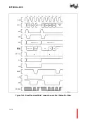
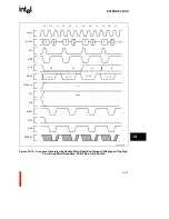
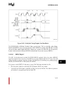
Figure 14-12
is a timing waveform of a read cycle followed by a write cycle, with an extra
recovery state inserted into the read cycle.
Содержание i960 Jx
Страница 1: ...Release Date December 1997 Order Number 272483 002 i960 Jx Microprocessor Developer s Manual ...
Страница 24: ......
Страница 25: ...1 INTRODUCTION ...
Страница 26: ......
Страница 35: ...2 DATA TYPES AND MEMORY ADDRESSING MODES ...
Страница 36: ......
Страница 46: ......
Страница 47: ...3 PROGRAMMING ENVIRONMENT ...
Страница 48: ......
Страница 73: ...4 CACHE AND ON CHIP DATA RAM ...
Страница 74: ......
Страница 85: ...5 INSTRUCTION SET OVERVIEW ...
Страница 86: ......
Страница 111: ...6 INSTRUCTION SET REFERENCE ...
Страница 112: ......
Страница 195: ...INSTRUCTION SET REFERENCE 6 83 6 Opcode mov 5CCH REG movl 5DCH REG movt 5ECH REG movq 5FCH REG See Also LOAD STORE lda ...
Страница 233: ...7 PROCEDURE CALLS ...
Страница 234: ......
Страница 256: ......
Страница 257: ...8 FAULTS ...
Страница 258: ......
Страница 291: ...9 TRACING AND DEBUGGING ...
Страница 292: ......
Страница 309: ...10 TIMERS ...
Страница 310: ......
Страница 324: ......
Страница 325: ...11 INTERRUPTS ...
Страница 326: ......
Страница 369: ...12 INITIALIZATION AND SYSTEM REQUIREMENTS ...
Страница 370: ......
Страница 412: ......
Страница 413: ...13 MEMORY CONFIGURATION ...
Страница 414: ......
Страница 429: ...14 EXTERNAL BUS ...
Страница 430: ......
Страница 468: ......
Страница 469: ...15 TEST FEATURES ...
Страница 470: ......
Страница 493: ...A CONSIDERATIONS FOR WRITING PORTABLE CODE ...
Страница 494: ......
Страница 502: ......
Страница 503: ...B OPCODES AND EXECUTION TIMES ...
Страница 504: ......
Страница 515: ...C MACHINE LEVEL INSTRUCTION FORMATS ...
Страница 516: ......
Страница 523: ...D REGISTER AND DATA STRUCTURES ...
Страница 524: ......
Страница 550: ......
Страница 551: ...GLOSSARY ...
Страница 552: ......
Страница 561: ...INDEX ...
Страница 562: ......
Страница 578: ......


