TIMERS
10-9
10
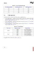
10.2.2
Load/Store Access Latency for Timer Registers
As with all other load accesses from internal memory-mapped registers, a load instruction that
accesses a timer register has a latency of one internal processor cycle. With one exception, a store
access to a timer register completes and all state changes take effect before the next instruction
begins execution. The exception to this is when disabling a timer. Latency associated with the
disabling action is such that a timer interrupt may be posted immediately after the disabling
instruction completes. This can occur when the timer is near zero as the store to TMRx occurs. In
this case, the timer interrupt is posted immediately after the store to TMRx completes and before
the next instruction can execute.
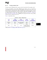
Table 10-5
summarizes the timer access and response timings.
Refer also to the individual register descriptions for details.
Note that the processor may delay the actual issuing of the load or store operation due to previous
instruction activity and resource availability of processor functional units.
The processor ensures that the TMRx.tc bit is cleared within one bus clock after a load or store
instruction accesses TMRx.
Table 10-5. Timer Responses to Register Bit Settings
(Sheet 1 of 2)
Name
Status
Action
(TMRx.tc)
Terminal Count
Bit 0
READ
Timer clears this bit when user software accesses TMRx. This bit can
be set 1 bus clock later. The timer sets this bit within 1 bus clock of
TCRx reaching zero when TMRx.reload=0.
WRITE
Timer clears this bit within 1 bus clock after the software accesses
TMRx. The timer ignores any value specified for TMRx.tc in a write
request.
(TMRx.enable)
Timer Enable
Bit 1
READ
Bit is available 1 bus clock after executing a read instruction from
TMRx.
WRITE
Writing a ‘1’ enables the bus clock to decrement TCRx within 1 bus
clock after executing a store instruction to TMRx.
(TMRx.reload)
Timer Auto
Reload Enable
Bit 2
READ
Bit is available 1 bus clock after executing a read instruction from
TMRx.
WRITE
Writing a ‘1’ enables the reload capability within 1 bus clock after the
store instruction to TMRx has executed. The timer loads TRRx data
into TCRx and decrements this value during the next bus clock cycle.
Содержание i960 Jx
Страница 1: ...Release Date December 1997 Order Number 272483 002 i960 Jx Microprocessor Developer s Manual ...
Страница 24: ......
Страница 25: ...1 INTRODUCTION ...
Страница 26: ......
Страница 35: ...2 DATA TYPES AND MEMORY ADDRESSING MODES ...
Страница 36: ......
Страница 46: ......
Страница 47: ...3 PROGRAMMING ENVIRONMENT ...
Страница 48: ......
Страница 73: ...4 CACHE AND ON CHIP DATA RAM ...
Страница 74: ......
Страница 85: ...5 INSTRUCTION SET OVERVIEW ...
Страница 86: ......
Страница 111: ...6 INSTRUCTION SET REFERENCE ...
Страница 112: ......
Страница 195: ...INSTRUCTION SET REFERENCE 6 83 6 Opcode mov 5CCH REG movl 5DCH REG movt 5ECH REG movq 5FCH REG See Also LOAD STORE lda ...
Страница 233: ...7 PROCEDURE CALLS ...
Страница 234: ......
Страница 256: ......
Страница 257: ...8 FAULTS ...
Страница 258: ......
Страница 291: ...9 TRACING AND DEBUGGING ...
Страница 292: ......
Страница 309: ...10 TIMERS ...
Страница 310: ......
Страница 324: ......
Страница 325: ...11 INTERRUPTS ...
Страница 326: ......
Страница 369: ...12 INITIALIZATION AND SYSTEM REQUIREMENTS ...
Страница 370: ......
Страница 412: ......
Страница 413: ...13 MEMORY CONFIGURATION ...
Страница 414: ......
Страница 429: ...14 EXTERNAL BUS ...
Страница 430: ......
Страница 468: ......
Страница 469: ...15 TEST FEATURES ...
Страница 470: ......
Страница 493: ...A CONSIDERATIONS FOR WRITING PORTABLE CODE ...
Страница 494: ......
Страница 502: ......
Страница 503: ...B OPCODES AND EXECUTION TIMES ...
Страница 504: ......
Страница 515: ...C MACHINE LEVEL INSTRUCTION FORMATS ...
Страница 516: ......
Страница 523: ...D REGISTER AND DATA STRUCTURES ...
Страница 524: ......
Страница 550: ......
Страница 551: ...GLOSSARY ...
Страница 552: ......
Страница 561: ...INDEX ...
Страница 562: ......
Страница 578: ......


