


EXTERNAL BUS
14-11
14
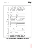
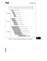
Figure 14-3
also shows a typical timing diagram for a non-burst, 32-bit write transaction. For the
write operation, W/R and DT/R are high to denote the direction of the data flow. The D/C pin is
high since instruction code cannot be written. During the Tw/Td state, the processor drives data on
the bus, waiting to sample RDYRCV low to terminate the transfer. The figure shows RDYRCV
assertion by external logic, so this state is a data state and the processor enters the recovery state.
At the end of a write, notice that the write data is driven during Tr and any subsequent Ti states.
After a write, the processor will drive write data until the next Ta state. See
section 14.2.4, “Bus
and Control Signals During Recovery and Idle States” (pg. 14-22)
for details.
14.2.3.3
Burst Transactions
A burst access is an address cycle followed by two to four data transfers. The i960 Jx micropro-
cessor uses burst transactions for instruction fetching and accessing system data structures.
Therefore, a system design incorporating an i960 Jx microprocessor must support burst transac-
tions. Burst accesses can also result from instruction references to data types which exceed the
width of the bus.
Maximum burst size is four data transfers, independent of bus width. A byte-wide bus has a
maximum burst size of four bytes; a word-wide bus has a maximum of four words. For an 8- or
16-bit bus, this means that some bus requests may result in multiple burst accesses. For example, if
a quad word load request (e.g., ldq instruction) is made to an 8-bit data region, it results in four,
4-byte, burst accesses. (See
Table 14-6 (pg. 14-23)
.
Burst accesses on a 32-bit bus are always aligned to even-word boundaries. Quad-word and
triple-word accesses always begin on quad-word boundaries (A3:2=00); double-word transfers
always begin on double-word boundaries (A2=0); single-word transfers occur on single word
boundaries.
Figure 14-4
shows burst, stop and start addresses for a 32-bit bus.
Содержание i960 Jx
Страница 1: ...Release Date December 1997 Order Number 272483 002 i960 Jx Microprocessor Developer s Manual ...
Страница 24: ......
Страница 25: ...1 INTRODUCTION ...
Страница 26: ......
Страница 35: ...2 DATA TYPES AND MEMORY ADDRESSING MODES ...
Страница 36: ......
Страница 46: ......
Страница 47: ...3 PROGRAMMING ENVIRONMENT ...
Страница 48: ......
Страница 73: ...4 CACHE AND ON CHIP DATA RAM ...
Страница 74: ......
Страница 85: ...5 INSTRUCTION SET OVERVIEW ...
Страница 86: ......
Страница 111: ...6 INSTRUCTION SET REFERENCE ...
Страница 112: ......
Страница 195: ...INSTRUCTION SET REFERENCE 6 83 6 Opcode mov 5CCH REG movl 5DCH REG movt 5ECH REG movq 5FCH REG See Also LOAD STORE lda ...
Страница 233: ...7 PROCEDURE CALLS ...
Страница 234: ......
Страница 256: ......
Страница 257: ...8 FAULTS ...
Страница 258: ......
Страница 291: ...9 TRACING AND DEBUGGING ...
Страница 292: ......
Страница 309: ...10 TIMERS ...
Страница 310: ......
Страница 324: ......
Страница 325: ...11 INTERRUPTS ...
Страница 326: ......
Страница 369: ...12 INITIALIZATION AND SYSTEM REQUIREMENTS ...
Страница 370: ......
Страница 412: ......
Страница 413: ...13 MEMORY CONFIGURATION ...
Страница 414: ......
Страница 429: ...14 EXTERNAL BUS ...
Страница 430: ......
Страница 468: ......
Страница 469: ...15 TEST FEATURES ...
Страница 470: ......
Страница 493: ...A CONSIDERATIONS FOR WRITING PORTABLE CODE ...
Страница 494: ......
Страница 502: ......
Страница 503: ...B OPCODES AND EXECUTION TIMES ...
Страница 504: ......
Страница 515: ...C MACHINE LEVEL INSTRUCTION FORMATS ...
Страница 516: ......
Страница 523: ...D REGISTER AND DATA STRUCTURES ...
Страница 524: ......
Страница 550: ......
Страница 551: ...GLOSSARY ...
Страница 552: ......
Страница 561: ...INDEX ...
Страница 562: ......
Страница 578: ......