B-1
APPENDIX B
INPUT SYNCHRONIZATION
Many input signals to an embedded processor are asynchronous. Asynchronous signals do not re-
quire a specified setup or hold time to ensure the device does not incur a failure. However, asyn-
chronous setup and hold times are specified in the data sheet to ensure recognition. Associated
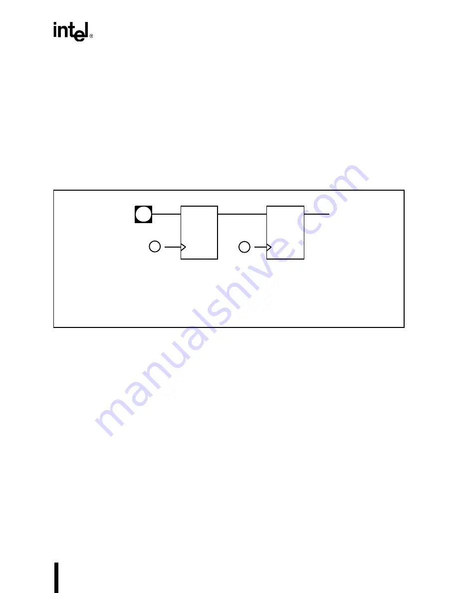
with each of these inputs is a synchronizing circuit (see Figure B-1) that samples the asynchro-
nous signal and synchronizes it to the internal operating clock. The output of the synchronizing
circuit is then safely routed to the logic units.
Figure B-1. Input Synchronization Circuit
B.1 WHY SYNCHRONIZERS ARE REQUIRED
Every data latch requires a specific setup and hold time to operate properly. The duration of the
setup and hold time defines a window during which the device attempts to latch the data. If the
input makes a transition within this window, the output may not attain a stable state. The data
sheet specifies a setup and hold window larger than is actually required. However, variations in
device operation (e.g., temperature, voltage) require that a larger window be specified to cover
all conditions.
Should the input to the data latch make a transition during the sample and hold window, the out-
put of the latch eventually attains a stable state. This stable state must be attained before the sec-
ond stage of synchronization requires a valid input. To synchronize an asynchronous signal, the
circuit in Figure B-1 samples the input into the first latch, allows the output to stabilize, then sam-
ples the stabilized value into a second latch. With the asynchronous signal resolved in this way,
the input signal cannot cause an internal device failure.
D
Q
D
Q
Synchronized
Output
Asynchronous
Input
1. First latch sample clock, can be phase 1 or phase 2 depending on pin function.
2. Second latch sample clock, opposite phase of first latch sample clock
(e.g., if first latch is sampled with phase 1, the second latch is sampled with phase 2).
First
Latch
Second
Latch
NOTES:
2
1
A1007-0A
Содержание 80C186EA
Страница 1: ...80C186EA 80C188EA Microprocessor User s Manual...
Страница 2: ...80C186EA 80C188EA Microprocessor User s Manual 1995...
Страница 19: ......
Страница 20: ...1 Introduction...
Страница 21: ......
Страница 28: ...2 Overview of the 80C186 Family Architecture...
Страница 29: ......
Страница 79: ......
Страница 80: ...3 Bus Interface Unit...
Страница 81: ......
Страница 129: ......
Страница 130: ...4 Peripheral Control Block...
Страница 131: ......
Страница 139: ......
Страница 140: ...5 ClockGenerationand Power Management...
Страница 141: ......
Страница 165: ......
Страница 166: ...6 Chip Select Unit...
Страница 167: ......
Страница 190: ...7 Refresh Control Unit...
Страница 191: ......
Страница 205: ......
Страница 206: ...8 Interrupt Control Unit...
Страница 207: ......
Страница 239: ...INTERRUPT CONTROL UNIT 8 32...
Страница 240: ...9 Timer Counter Unit...
Страница 241: ......
Страница 265: ......
Страница 266: ...10 Direct Memory Access Unit...
Страница 267: ......
Страница 295: ...DIRECT MEMORY ACCESS UNIT 10 28...
Страница 296: ...11 Math Coprocessing...
Страница 297: ......
Страница 314: ...12 ONCE Mode...
Страница 315: ......
Страница 318: ...A 80C186 Instruction Set Additions and Extensions...
Страница 319: ......
Страница 330: ...B Input Synchronization...
Страница 331: ......
Страница 334: ...C Instruction Set Descriptions...
Страница 335: ......
Страница 383: ...INSTRUCTION SET DESCRIPTIONS C 48...
Страница 384: ...D Instruction Set Opcodes and Clock Cycles...
Страница 385: ......
Страница 408: ...Index...
Страница 409: ......


