5-23
CLOCK GENERATION AND POWER MANAGEMENT
5.2.4 Implementing a Power Management Scheme
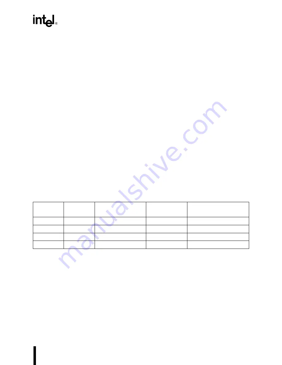
Table 5-2 summarizes the power management options available to the user. With three ways
available to reduce power consumption, here are some guidelines:
•
Powerdown mode reduces power consumption by several orders of magnitude. If the
application goes into and out of Powerdown frequently, the power reduction can probably
offset the relatively long intervals spent leaving Powerdown mode.
•
If background CPU tasks are usually necessary and the overhead of reprogramming
peripherals is not severe, Power-Save mode can “tune” the clock rate to the best value.
Remember that current varies linearly with respect to frequency.
•
Idle mode fits DMA-intensive and interrupt-intensive (as opposed to CPU-intensive) appli-
cations perfectly.
The processor can operate in Power-Save mode and Idle mode concurrently. With Idle mode
alone, rated power consumption typically drops a third or more. Power-Save mode multiplies that
reduction further according to the selected clock divisor.
Overall power consumption has two parts: switching power dissipated by driving loads such as
the address/data bus, and device power dissipated internally by the microprocessor whether or not
it is connected to external devices. A power management scheme should consider loading as well
as the raw specifications in the processor's data sheet.
NOTE
If an NMI or external maskable interrupt service routine is used to enter a
power management mode, the interrupt request signal should be deasserted
before entering the power management mode.
Table 5-2. Summary of Power Management Modes
Mode
Relative
Power
Typical
Power
User
Overhead
Chief
Advantage
Active
Full
250 mW at 16 MHz
—
Full-speed operation
Idle
Low
175 mW at 16 MHz
Low
Peripherals are unaffected
Power-Save
Adjustable
125 mW at 16/2 MHz
Moderate to High
Code execution continues
Powerdown
Lowest
250 µW
Low to Moderate
Long battery life
Содержание 80C186EA
Страница 1: ...80C186EA 80C188EA Microprocessor User s Manual...
Страница 2: ...80C186EA 80C188EA Microprocessor User s Manual 1995...
Страница 19: ......
Страница 20: ...1 Introduction...
Страница 21: ......
Страница 28: ...2 Overview of the 80C186 Family Architecture...
Страница 29: ......
Страница 79: ......
Страница 80: ...3 Bus Interface Unit...
Страница 81: ......
Страница 129: ......
Страница 130: ...4 Peripheral Control Block...
Страница 131: ......
Страница 139: ......
Страница 140: ...5 ClockGenerationand Power Management...
Страница 141: ......
Страница 165: ......
Страница 166: ...6 Chip Select Unit...
Страница 167: ......
Страница 190: ...7 Refresh Control Unit...
Страница 191: ......
Страница 205: ......
Страница 206: ...8 Interrupt Control Unit...
Страница 207: ......
Страница 239: ...INTERRUPT CONTROL UNIT 8 32...
Страница 240: ...9 Timer Counter Unit...
Страница 241: ......
Страница 265: ......
Страница 266: ...10 Direct Memory Access Unit...
Страница 267: ......
Страница 295: ...DIRECT MEMORY ACCESS UNIT 10 28...
Страница 296: ...11 Math Coprocessing...
Страница 297: ......
Страница 314: ...12 ONCE Mode...
Страница 315: ......
Страница 318: ...A 80C186 Instruction Set Additions and Extensions...
Страница 319: ......
Страница 330: ...B Input Synchronization...
Страница 331: ......
Страница 334: ...C Instruction Set Descriptions...
Страница 335: ......
Страница 383: ...INSTRUCTION SET DESCRIPTIONS C 48...
Страница 384: ...D Instruction Set Opcodes and Clock Cycles...
Страница 385: ......
Страница 408: ...Index...
Страница 409: ......


