1 OVeRVieW
S1C17624/604/622/602/621 TeChniCal Manual
Seiko epson Corporation
1-1
Overview
1
The S1C17624/604/622/602/621 is a 16-bit MCU featuring high-speed low-power operations, compact dimensions,
wide address space, and on-chip ICE. Based on an S1C17 CPU core, this product consists of a Flash memory,
RAM, serial interface modules supporting sensors such as UART to support high-bit rate and IrDA1.0, SPI, and
I
2
C, various timers, maximum 47 general input/output ports, maximum 52 segment
×
8 common LCD driver and a
power supply voltage booster circuit, A/D converter, R/F converter, supply voltage detector, and 32 kHz and maxi-
mum 8.2 MHz oscillator circuits.
It allows 8.2 MHz high-speed operation at a minimum of 1.8 V operating voltage, and executes a basic instruction
in one clock cycle with 16-bit RISC processing. The S1C17624/604/622/602/621 also includes a coprocessor sup-
porting multiplication, division, and MAC (multiply and accumulation) operations.
The on-chip ICE function allows onboard Flash programming/erasing, program debugging, and evaluations using
the ICDmini (S5U1C17001H) that can be connected with three signal wires.
The S1C17624/604/622/602/621 is ideal for applications, such as health care products with sensors, sports watches,
and meter modules that must be driven with battery power and require sensor interfaces and a high-definition LCD
display.
Features
1.1
The main features of the S1C17624/604/622/602/621 are listed below.
1.1 Features
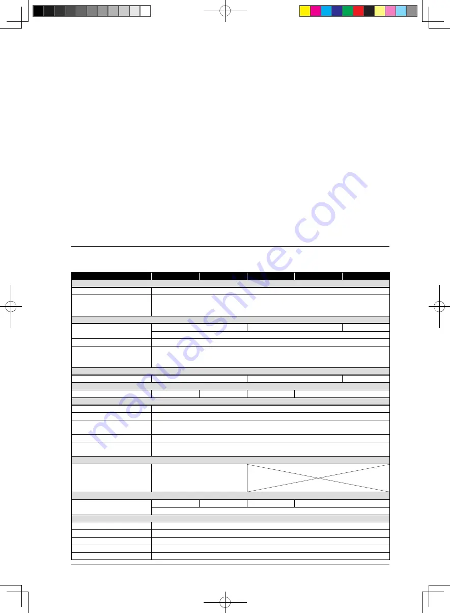
Table 1.
Model
S1C17624
S1C17604
S1C17622
S1C17602
S1C17621
CPu
CPU core
Seiko Epson original 16-bit RISC CPU core S1C17
Multiplier/Divider (COPRO)
• 16-bit
×
16-bit multiplier
• 16-bit
×
16-bit + 32-bit multiply and accumulation unit
• 16-bit
÷
16-bit divider
embedded Flash memory
Capacity
128K bytes
64K bytes
32K bytes
(Can be used for both instructions and data.)
Erase/program count
1,000 cycles (min.)
Other
• Read/program protection function
• Allows on-board programming using a debugging tool such as ICDmini (S5U1C17001H) and self-
programming by software control.
embedded RaM
Capacity
8K bytes
4K bytes
2K bytes
embedded Display RaM
Capacity
56 bytes
40 bytes
56 bytes
40 bytes
Clock generator
System clock source
3 sources (IOSC/OSC3/OSC1)
IOSC oscillator circuit
2.7 MHz(typ.) internal oscillator circuit (oscillation start time 5 µs min.)
OSC3 oscillator circuit
8.2 MHz (max.) crystal or ceramic oscillator circuit
Supports an external clock input.
OSC1 oscillator circuit
32.768 kHz (typ.) crystal oscillator circuit
Other
• Core clock frequency control
• Peripheral module clock supply control
Real-time clock
RTC module
Included
(Contains second, minute, hour,
day, days of week, month, and year
counters.)
i/O ports
Number of general-purpose I/O
ports
Max. 47 bits
Max. 36 bits
Max. 47 bits
Max. 36 bits
(Pins are shared with the peripheral I/O.)
Serial interfaces
SPI
1 channel
I
2
C master (I2CM)
1 channel
I
2
C slave (I2CS)
1 channel
UART
2 channels (IrDA1.0 supported)
IR remote controller (REMC)
1 channel


