


- 20 -
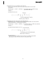
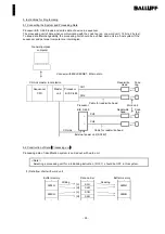
(2) Data store format of code tag "memory"
<
>
<
>
Writing data
Code tag "memory"
Word address
0H
[
]
Word data
Write to word address
0H
1
2
E
F
E
F
1
2
byte address 0H
1H
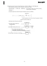
(3) Setting of block
Set block No. with dip switch.
Refer to "4.3 Each part and setting" for setting.
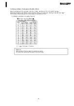
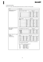
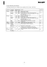
3.5 Data processing time
Processing time for read and write data is indicated in following table.
(
)
(
)
Code tag 32 byte
Code tag 64 byte
Data number
Processing time
Data number
Processing time
word
byte
reading
writing
word
byte
reading
writing
1
2
0.2sec
0.35sec
1
2
0.4sec
0.65sec
50
100
0.7sec
2.3sec
50
100
0.7sec
2.3sec
100
200
1.4sec
4.3sec
100
200
1.4sec
4.3sec
150
300
2.1sec
6.2sec
150
300
2.1sec
6.2sec
200
400
2.8sec
8.6sec
200
400
2.8sec
8.6sec
250
500
3.5sec
11.0sec
250
500
3.5sec
11.0sec
300
600
4.2sec
12.1sec
300
600
4.2sec
12.1sec
350
700
4.9sec
14.2sec
350
700
4.9sec
14.2sec
400
800
5.6sec
17.3sec
400
800
5.6sec
17.3sec
450
900
6.3sec
19.5sec
450
900
6.3sec
19.5sec
500
1000
7.0sec
21.5sec
500
1000
7.0sec
21.5sec
512
1024
7.2sec
21.9sec
512
1024
7.2sec
21.9sec
(note 1) Processing time is the time that processing takes for each data consecutively.
(note 2) Processing time is the time since "request communication" turns "ON" until "finish ID instruction" turns "ON".
(note 3) The condition of measurement : connect 1 processor (occupied 4 stations) to master unit, with read/write heads
on 2 channels.
It is including link scan time-and time delay of transmission.
Refer to user's manual for master local unit on the detail of link scan time, time delay of transmission.
Содержание BIS C-489-1 KBT02 Series
Страница 7: ... 4 2 3 Dimension ...