Chapter 4 Operations for Each Function
4-66
Waveform
memory
DA converter
14
14
Vector
modulator
Pulse
modulator
3
Markers 1, 2, 3
RF Gate
Delay
3
Waveform data
Sample 2
Sample 1
RF Gate
Sample 3
Sample 4
1
0
1
0
RF output
ON
OFF
ON
ON
Waveform data, 14 bits
×
2 ch
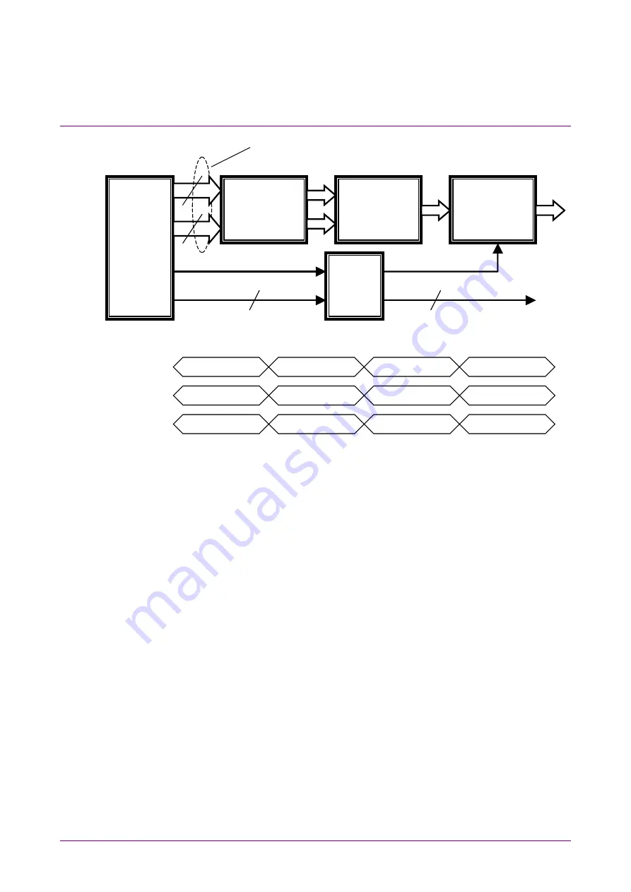
Figure 4.5.6-4 Waveform Pattern Generator Block Diagram and Output Signal Timing Chart of
Mainframe


