DBS9900 User’s Manual
DBS9900 Clock
7-19
82-28993 Revision 01
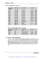
Table 23 – DAC Codes
DAC Code
Analog Output
FF
+9.921875
81
+78.125mV
80
0V
7F
-78.125mV
01
-9.921875V
00
-10.0V
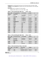
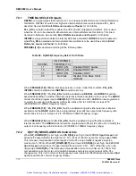
Table 24 - Clock A Threshold Register Map Base + 0x14
Base + 0X14
Clock A
Register Map
Default
Data Bus
Function
D[07]
CLKA_THRESH[7] , MSB
Set to 0
R/W
D[06]
CLKA_THRESH[6]
Set to 0
R/W
D[05]
CLKA_THRESH[5]
Set to 0
R/W
D[04]
CLKA_THRESH[4]
Set to 0
R/W
D[03]
CLKA_THRESH[3]
Set to 0
R/W
D[02]
CLKA_THRESH[2]
Set to 0
R/W
D[01]
CLKA_THRESH[1]
Set to 0
R/W
D[00]
CLKA_THRESH[0], LSB
Set to 0
R/W
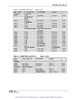
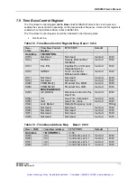
Table 25 - Time Base Address Map Base + 0x18 (8h)
Base + 0X18
Time Base Address FUNCTION
Default
Data Bus
TB CONTROL
C=8h
D[03]
C[4]
Control bit, set to 1
Set to 0
R/W
D[02]
C[3]
Control bit, set to 0
Set to 0
R/W
D[01]
C[2]
Control bit, set to 0
Set to 0
R/W
D[00]
C[1]
Control bit, set to 0
Set to 0
R/W
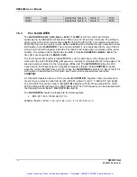
7.12 Clock B Threshold Register
The Clock B Threshold Register
(0x14, Base + 0x18 = 9h)
R/W,
stores the bits needed to set the
Clock B zero crossing thresholds. The byte,
D[07:00]
contains programming bits for clock B zero
crossing. To access this register, the software driver writes to the control bits located in
Base +
0x18 = 9h
of the VXI FPGA. This register instructs the FPGA that the next register writes the
Clock B Threshold Register
at
0x14
. The zero crossing of the clock threshold is set by
programming one of four DAC’s in a quad 8 bit DAC to a voltage, from –10V to +9.921875V in
78.125mV steps. The coding is offset binary and the code map is as follows:
Artisan Technology Group - Quality Instrumentation ... Guaranteed | (888) 88-SOURCE | www.artisantg.com

