


DBS9900 User’s Manual
DBS9900 Clock
7-1
82-28993 Revision 01
7 Clock
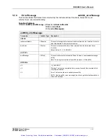
7.1 Channel A/B Clock Selection:
The DBS9900 has two clock inputs: Channel A and Channel B. Each channel enters the
DBS9900 through a non-isolated SMA connector on the front panel and is routed to a high speed
comparator. The threshold can be programmed to any voltage between –10V and +9.921875V
with 8 bit resolution. There is a fixed 40mV hysteresis built into the input of the comparators to
prevent inadvertent pulses from noisy inputs. Each comparator output is routed to a 4:1 Mux
which select no clock, Time Base Clock, Channel A input or Channel B input clock. The output of
the Channel B comparator is also routed to a 2:1 Mux which selects either a internal 10MHz
reference oscillator (default) or the Channel B input. This allows the connection of an external
10MHz reference clock to the PLL reference input. This allows multiple daughter boards to run off
of one reference, being synchronized together.
Since the input impedance is 4k
Ω
, it is expected that the user will source terminate their drivers
with 50
Ω
series terminators to prevent reflections.
7.2 Frequency Synthesizer:
The internal clock generation circuitry consists of a 550MHz Phase Lock Loop (National
LMX2306), which is programmed to generate frequencies (
Fvco
) from 100MHz to 200MHz in
50kHz steps. The wide adjustment range (over two to one) is achieved by a wide frequency range
voltage controlled oscillator (Mini-Circuits JTOS-200). A 10MHz, 25PPM accurate crystal
oscillator is used as a reference input to the PLL.
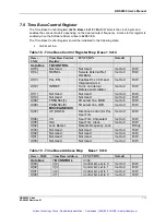
7.3 Time Base Divider:
The internal synthesizer drives a 2-tiered clock divider chain consisting of high and low speed
divider elements to give frequency division ratios from 2 to 1,048,592. The high-speed divider
(
HSDIV
) provides time base clock division ratios of 2 to 32 in steps of two. The low-speed divider
(
LSDIV
) provides clock division ratios of 32 to 1,048,592, in steps of 16. The synthesizer/time
base is able to generate sample rates from 95.36598Hz to 100MHz, with a worst case resolution
of 500PPM of the programmed frequency. The lower divider chain is turned on only as needed in
order to keep sub-harmonic beat frequencies out of the clock signal. A 4:1 Mux selects no clock,
LSDIV Clock, HSDIV Clock. This clock (
TBCLOCK
) is routed to the daughter board clock
selection muxes, which in turn are routed to the daughter board, and the trigger FPGA controller.
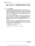
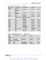
7.4 Program Sequence:
The programming model should look like the following process:
Program PLL:
•
Program R-COUNTER (0x18, = 0h, 0x14, 0x16).
•
Program N-COUNTER (0x18 = 1h, 0x14, 0x16).
•
Program FUNCTION LATCH (0x18 = 2h or 3h, 0x14, 0x16)
Artisan Technology Group - Quality Instrumentation ... Guaranteed | (888) 88-SOURCE | www.artisantg.com


