Major Chips Description
2-41
The C&T65550 offers a variety of programmable features to optimize display quality. Vertical
centering and stretching are provided for handling modes with less than 480 lines on 480-line
panels. Horizontal and vertical stretching capabilities are also available for both text and graphics
modes for optimal display of VGA text and graphics modes on 800x600 and 1024x768 panels.
Three selectable color-to-gray scale reduction techniques and SMARTMAP™ are available for
improving the ability to view color applications on monochrome panels. CHIPS' polynomial FRC
algorithm reduces panel flicker on a wider range of panel types with a single setting for a particular
panel type.
LOW POWER CONSUMPTION
The C&T65550 employs a variety of advanced power management features to reduce power
consumption of the display sub-system and extend battery life. Although optimized for 3.3V
operation, The C&T65550 controller's internal logic. memory interface, bus interface, and panel
interfaces can he independently configured to operate at either 3.3V or 5V.
SOFTWARE COMPATIBILITY/FLEXIBILITY
The C&T65550 are fully compatible with VGA at the register, and BIOS levels. CHIPS and third-
party vendors supply fully VGA-compatible BIOS, end-user utilities and drivers for common
application programs
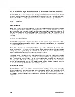
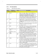
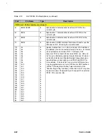
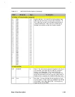
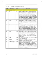
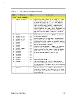
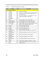
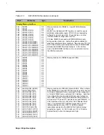
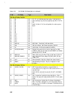
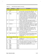
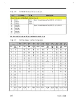
Pin names in parentheses (...) indicate alternate functions.
2.5.2
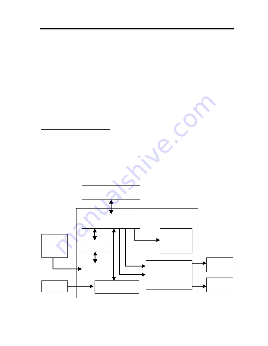
Block Diagram
Memory Controller
Scaling
Capture
64-bit
Graphics
Engine
YUV to RGB
Color Key Zoom
Bus Interface
Video
Capture
Port
PCI Bus
Analog
RGB
Digital
RGB
Video Memory
Figure 2-9
C&T 65550 Block Diagram
Содержание Extensa 61X
Страница 1: ...TI Extensa 61X Series AcerNote 370P Notebook Service Guide PART NO 2238309 0809 DOC NO PRINTED IN USA ...
Страница 6: ...vi ...
Страница 26: ...1 8 Service Guide Figure 1 5 Main Board Layout Bottom Side ...
Страница 49: ...System Introduction 1 31 1 5 1 3 Power Management Figure 1 14 Power Management Block Diagram ...
Страница 55: ...System Introduction 1 37 1 6 System Block Diagram Figure 1 15 System Block Diagram ...
Страница 64: ...Major Chips Description 2 7 2 2 5 Pin Diagram Figure 2 4 M1521 Pin Diagram ...
Страница 99: ...2 42 Service Guide 2 5 3 Pin Diagram Figure 2 10 C T 65550 Pin Diagram ...
Страница 116: ...Major Chips Description 2 59 2 6 4 Block Diagram Figure 2 11 Functional Block Diagram 16 bit PC Card Interface ...
Страница 117: ...2 60 Service Guide Figure 2 12 Functional block diagram CardBus Card Interface ...
Страница 118: ...Major Chips Description 2 61 2 6 5 Pin Diagram Figure 2 13 PCI to PC Card 16 bit terminal assignments ...
Страница 119: ...2 62 Service Guide Figure 2 14 PCI to CardBus terminal assignments ...
Страница 135: ...2 78 Service Guide 2 7 3 Pin Diagram Figure 2 16 NS87336VJG Pin Diagram ...
Страница 145: ...2 88 Service Guide 2 8 2 Pin Diagram Figure 2 17 YMF715 Block Diagram ...
Страница 185: ...Disassembly and Unit Replacement 4 5 Figure 4 3 Disassembly Sequence Flowchart ...
Страница 209: ...B 2 Service Guide ...
Страница 210: ...Exploded View Diagram B 3 ...
Страница 217: ...A p p e n d i x D A p p e n d i x D Schematics This appendix shows the schematic diagrams of the notebook ...


