Major Chips Description
2-43
2.5.4
Pin Descriptions
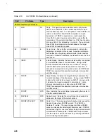
Table 2-10
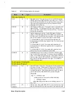
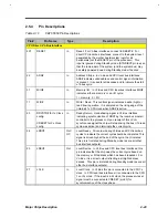
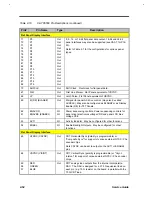
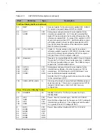
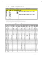
C&T 65550 Pin Descriptions
Pin#
Pin Name
Type
Description
CPU Direct / VL-Bus Interface
207
RESET
In
Reset. For VL-Bus interfaces, connect to RESET#. For
direct CPU local bus interfaces, connect to the system reset
generated by the mother board system logic for all
peripherals (not the RESET# pin of the processor). This
input is ignored during Standby mode (STNDIBY# pin low) so
that the remainder of the system (and the system bus) may
be safely powered down during Standby mode if desired.
22
ADS#
In
Address Strobe. In VL-Bus and CPU local bus interfaces
ADS# indicates valid address and control signal information
is present. It is used for all decodes and to indicate the start
of a bus cycle.
31
M/IO#
In
Memory /IO. In VL-Bus and CPU local bus interfaces M/lO#
indicates either a memory or an I/O cycle:
1 = memory, 0 = I/O
11
W/R#
In
Write / Read. This control signal indicates a write (high) or
read (low) operation. It is sampled on the rising edge of the
(internal) 1x CPU clock when ADS# is active.
23
RDYRTN# for 1x Clock
config
CRESET for 2x Clock
config
In
Ready Return. Handshaking signal in VL-Bus interface
indicating synchronization of RDY# by the local bus master /
controller to the processor. Upon receipt of this LCLK-
synchronous signal the chip will stop driving the bus (if a read
cycle was active) and terminate the current cycle.
24
LRDY#
Out/
OC
Local Ready. Driven low during VL-Bus and CPU local bus
cycles to indicate the current cycle should be completed This
signal is driven high at the end of the cycle, then tri-stated.
This pin is tri-stated during Standby mode (as are all other
bus interface outputs).
25
LDEV#
Out
Local Device. In VL Bus and CPU local bus interfaces. this
pin indicates that the chip owns the current cycle based on
the memory or l/O address which has been broadcast. For
VL-Bus, it is a direct output reflecting a straight address
decode. This pin is tri-stated during Standby mode (as are all
other bus interface outputs).
27
LCLK
In
Local Clock. In VL Bus this pin is connected to the CPU 1x
clock. In CPU local bus interfaces it is connected to the CPU
1x or 2x clock. If the input is a 2x clock, the processor reset
signal must be connected to CRESET (pin 23) for
synchronization of the clock phase.
Содержание Extensa 61X
Страница 1: ...TI Extensa 61X Series AcerNote 370P Notebook Service Guide PART NO 2238309 0809 DOC NO PRINTED IN USA ...
Страница 6: ...vi ...
Страница 26: ...1 8 Service Guide Figure 1 5 Main Board Layout Bottom Side ...
Страница 49: ...System Introduction 1 31 1 5 1 3 Power Management Figure 1 14 Power Management Block Diagram ...
Страница 55: ...System Introduction 1 37 1 6 System Block Diagram Figure 1 15 System Block Diagram ...
Страница 64: ...Major Chips Description 2 7 2 2 5 Pin Diagram Figure 2 4 M1521 Pin Diagram ...
Страница 99: ...2 42 Service Guide 2 5 3 Pin Diagram Figure 2 10 C T 65550 Pin Diagram ...
Страница 116: ...Major Chips Description 2 59 2 6 4 Block Diagram Figure 2 11 Functional Block Diagram 16 bit PC Card Interface ...
Страница 117: ...2 60 Service Guide Figure 2 12 Functional block diagram CardBus Card Interface ...
Страница 118: ...Major Chips Description 2 61 2 6 5 Pin Diagram Figure 2 13 PCI to PC Card 16 bit terminal assignments ...
Страница 119: ...2 62 Service Guide Figure 2 14 PCI to CardBus terminal assignments ...
Страница 135: ...2 78 Service Guide 2 7 3 Pin Diagram Figure 2 16 NS87336VJG Pin Diagram ...
Страница 145: ...2 88 Service Guide 2 8 2 Pin Diagram Figure 2 17 YMF715 Block Diagram ...
Страница 185: ...Disassembly and Unit Replacement 4 5 Figure 4 3 Disassembly Sequence Flowchart ...
Страница 209: ...B 2 Service Guide ...
Страница 210: ...Exploded View Diagram B 3 ...
Страница 217: ...A p p e n d i x D A p p e n d i x D Schematics This appendix shows the schematic diagrams of the notebook ...

