2-14
Service Guide
2.3
ALI M1523
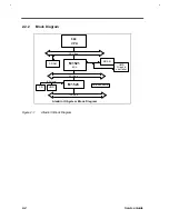
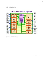
The M1523 is a bridge between PCI and ISA bus, providing full PCI and ISA compatible functions.
The M1523 has Integrated System Peripherals (ISP) on-chip and provides advanced features in
the DMA controller. This chip contains the keyboard controller, real-time clock and IDE master
controller. This chip also supports the Advanced Programmable Interrupt controller (APIC)
interface.
One eight-byte bidirectional line buffer is provided for ISA/DMA master memory read/writes. One
32-bit wide posted-write buffer is provided for PCI memory write cycles to the ISA bus. It also
supports a PCI to ISA IRQ routing table and level-to-edge trigger transfer.
The chip has two extra IRQ lines and one programmable chip select for motherboard Plug-and-
Play functions. The interrupt lines can be routed to any of the available ISA interrupts.
The on-chip IDE controller supports two IDE connectors for up to four IDE devices providing an
interface for IDE hard disks and CD-ROMs. The ATA bus pins are dedicated to improve the
performance of IDE master.
The M1523 supports the Super Green feature for Intel and Intel compatible CPUs. It implements
programmable hardware events, software event and external switches (for suspend/turbo/ring-in).
The M1523 provides CPU clock control (STPCLKJ). The STPCLKJ can be active (low) or inactive
(high) in turn by throttling control.
2.3.1
Features
•
Technology
•
0.6µm, triple-metal CMOS process
•
Provides a bridge between the PCI bus and ISA bus
•
PCI interface
•
Supports PCI master and slave interface
•
Supports PCI master and slave initiated termination
•
PCI spec. 2.1 compliant (delay transaction support)
•
Buffers
•
8-byte bidirectional line buffers for DMA/ISA memory read/write cycles to PCI bus
•
32-bit posted-write buffer for PCI memory write and I/O data write (for sound card) to ISA
bus
•
Provides steerable PCI interrupts for PnP PCI devices
•
Up to eight PCI interrupts routing
•
Level-to-edge trigger transfer
•
Enhanced DMA controller
•
Provides seven programmable channels (four for 8-bit data size, three for 16-bit data
size)
Содержание Extensa 61X
Страница 1: ...TI Extensa 61X Series AcerNote 370P Notebook Service Guide PART NO 2238309 0809 DOC NO PRINTED IN USA ...
Страница 6: ...vi ...
Страница 26: ...1 8 Service Guide Figure 1 5 Main Board Layout Bottom Side ...
Страница 49: ...System Introduction 1 31 1 5 1 3 Power Management Figure 1 14 Power Management Block Diagram ...
Страница 55: ...System Introduction 1 37 1 6 System Block Diagram Figure 1 15 System Block Diagram ...
Страница 64: ...Major Chips Description 2 7 2 2 5 Pin Diagram Figure 2 4 M1521 Pin Diagram ...
Страница 99: ...2 42 Service Guide 2 5 3 Pin Diagram Figure 2 10 C T 65550 Pin Diagram ...
Страница 116: ...Major Chips Description 2 59 2 6 4 Block Diagram Figure 2 11 Functional Block Diagram 16 bit PC Card Interface ...
Страница 117: ...2 60 Service Guide Figure 2 12 Functional block diagram CardBus Card Interface ...
Страница 118: ...Major Chips Description 2 61 2 6 5 Pin Diagram Figure 2 13 PCI to PC Card 16 bit terminal assignments ...
Страница 119: ...2 62 Service Guide Figure 2 14 PCI to CardBus terminal assignments ...
Страница 135: ...2 78 Service Guide 2 7 3 Pin Diagram Figure 2 16 NS87336VJG Pin Diagram ...
Страница 145: ...2 88 Service Guide 2 8 2 Pin Diagram Figure 2 17 YMF715 Block Diagram ...
Страница 185: ...Disassembly and Unit Replacement 4 5 Figure 4 3 Disassembly Sequence Flowchart ...
Страница 209: ...B 2 Service Guide ...
Страница 210: ...Exploded View Diagram B 3 ...
Страница 217: ...A p p e n d i x D A p p e n d i x D Schematics This appendix shows the schematic diagrams of the notebook ...


