2-76
Service Guide
•
The Bidirectional Parallel Port:
•
Enhanced Parallel Port(EPP) compatible
•
Extended Capabilities Port(ECP) compatible, including level 2 support
•
Bidirectional under either software or hardware control
•
Compatible with ISA, and EISA, architectures
•
Ability to multiplex FDC signals on parallel port pins allows use of an external Floppy
Disk Drive(FDD)
•
Includes protection circuit to prevent damage to the parallel port when a connected
printer is powered up or is operated at a higher voltage
•
The UARTs:
•
Software compatible with the PC16550A and PC16450
•
MIDI baud rate support
•
Infrared support on UART2(IrDA and Sharp-compliant)
•
The Address Decoder
•
6 bit or 10 bit decoding
•
External Chip Select capability when 10 bit decoding
•
Full relocation capability(No limitation)
•
Enhanced Power Management
•
Special configuration registers for power-down
•
Enhanced programmable power-down FDC command
•
Auto power-down and wake-up modes
•
2 special pins for power management
•
Typical current consumption during power-down is less than 10 uA
•
Reduced pin leakage current
•
Mixed Voltage support
•
Supports standard 5V operation
•
Supports 3.3V operation
•
Supports mixed internal 3.3V operation with 3.3V/5V external configuration
•
The General Purpose Pins:
•
2 pins, for 2 separate programmable chip select decoders, can be programmed for game
port control
Содержание Extensa 61X
Страница 1: ...TI Extensa 61X Series AcerNote 370P Notebook Service Guide PART NO 2238309 0809 DOC NO PRINTED IN USA ...
Страница 6: ...vi ...
Страница 26: ...1 8 Service Guide Figure 1 5 Main Board Layout Bottom Side ...
Страница 49: ...System Introduction 1 31 1 5 1 3 Power Management Figure 1 14 Power Management Block Diagram ...
Страница 55: ...System Introduction 1 37 1 6 System Block Diagram Figure 1 15 System Block Diagram ...
Страница 64: ...Major Chips Description 2 7 2 2 5 Pin Diagram Figure 2 4 M1521 Pin Diagram ...
Страница 99: ...2 42 Service Guide 2 5 3 Pin Diagram Figure 2 10 C T 65550 Pin Diagram ...
Страница 116: ...Major Chips Description 2 59 2 6 4 Block Diagram Figure 2 11 Functional Block Diagram 16 bit PC Card Interface ...
Страница 117: ...2 60 Service Guide Figure 2 12 Functional block diagram CardBus Card Interface ...
Страница 118: ...Major Chips Description 2 61 2 6 5 Pin Diagram Figure 2 13 PCI to PC Card 16 bit terminal assignments ...
Страница 119: ...2 62 Service Guide Figure 2 14 PCI to CardBus terminal assignments ...
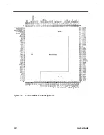
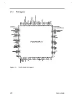
Страница 135: ...2 78 Service Guide 2 7 3 Pin Diagram Figure 2 16 NS87336VJG Pin Diagram ...
Страница 145: ...2 88 Service Guide 2 8 2 Pin Diagram Figure 2 17 YMF715 Block Diagram ...
Страница 185: ...Disassembly and Unit Replacement 4 5 Figure 4 3 Disassembly Sequence Flowchart ...
Страница 209: ...B 2 Service Guide ...
Страница 210: ...Exploded View Diagram B 3 ...
Страница 217: ...A p p e n d i x D A p p e n d i x D Schematics This appendix shows the schematic diagrams of the notebook ...

