Major Chips Description
2-65
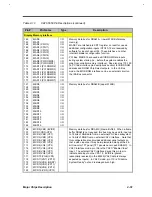
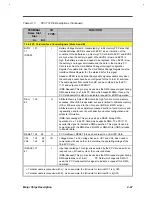
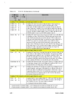
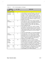
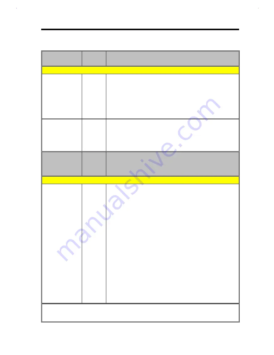
Table 2-13
PCI1131 Pin Descriptions (Continued)
TERMINAL
NAME NO.
I/O
TYPE
FUNCTION
PCI Interface Control Terminals
TRDY 196
I/O
Target ready. Indicates the PCI 1131 ability to complete the current
data phase of the transaction. TRDY is used in conjunction with IRDY.
A data phase is completed on any clock where both TRDY I/O are
sampled asserted. During a read, TRDY indicates that valid data is
present on AD31-0. During a write, TRDY indicates the PCI1131 is
prepared to accept data. Wait cycles are inserted until both TIRDY and
TRDY are asserted together. This signal is an output when the PCI
1131 is the PCI target. and an input when it is the PCI bus master.
IRQ10/CLKRUN
159
IRQ12/CLKRUN
161
I/O
Interrupt Request 10 and 12. This terminal is software configurable
and is used by the PCI 1131 to support the PCI Clock Run protocol.
When configured as CLKRUN, by setting bit 0 in the System Control
Register at offset 80h, this terminal is an open drain output. To select
between IRQ10 and IRQ12 as the output use bit 7 of Register 80h.
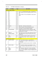
TERMINAL
Name Slot
Slot
I/O
TYPE
FUNCTION
A+ B
≠≠
1 6-bit PC Card Address and Data (Slots A and B)
A25 121 55
A24
118 53
A23
116 51
A22
114 49
A21
111 47
A20
109 45
A19
107 42
A18
105 40
A17
103 37
A16
112 48
A15
115 50
A14
108 43
A12
106 41
A11
100 34
A10
95 29
A9
102 36
A8
104 39
A7
119 54
A6
123 57
A5
125 59
A4
126 60
A3
128 62
A2
131 65
A 1
132 66
A0
133 67
O
PC Card Address. 16-bit PC Card address lines. A25 is the most
significant bit.
+
Terminal name is preceded with A_. As an example, the full name for terminal 121 is A_A25.
≠
Terminal name is preceded with B_. As an example, the full name for terminal 55 is B_A25.
Содержание Extensa 61X
Страница 1: ...TI Extensa 61X Series AcerNote 370P Notebook Service Guide PART NO 2238309 0809 DOC NO PRINTED IN USA ...
Страница 6: ...vi ...
Страница 26: ...1 8 Service Guide Figure 1 5 Main Board Layout Bottom Side ...
Страница 49: ...System Introduction 1 31 1 5 1 3 Power Management Figure 1 14 Power Management Block Diagram ...
Страница 55: ...System Introduction 1 37 1 6 System Block Diagram Figure 1 15 System Block Diagram ...
Страница 64: ...Major Chips Description 2 7 2 2 5 Pin Diagram Figure 2 4 M1521 Pin Diagram ...
Страница 99: ...2 42 Service Guide 2 5 3 Pin Diagram Figure 2 10 C T 65550 Pin Diagram ...
Страница 116: ...Major Chips Description 2 59 2 6 4 Block Diagram Figure 2 11 Functional Block Diagram 16 bit PC Card Interface ...
Страница 117: ...2 60 Service Guide Figure 2 12 Functional block diagram CardBus Card Interface ...
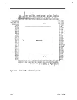
Страница 118: ...Major Chips Description 2 61 2 6 5 Pin Diagram Figure 2 13 PCI to PC Card 16 bit terminal assignments ...
Страница 119: ...2 62 Service Guide Figure 2 14 PCI to CardBus terminal assignments ...
Страница 135: ...2 78 Service Guide 2 7 3 Pin Diagram Figure 2 16 NS87336VJG Pin Diagram ...
Страница 145: ...2 88 Service Guide 2 8 2 Pin Diagram Figure 2 17 YMF715 Block Diagram ...
Страница 185: ...Disassembly and Unit Replacement 4 5 Figure 4 3 Disassembly Sequence Flowchart ...
Страница 209: ...B 2 Service Guide ...
Страница 210: ...Exploded View Diagram B 3 ...
Страница 217: ...A p p e n d i x D A p p e n d i x D Schematics This appendix shows the schematic diagrams of the notebook ...

