2-74
Service Guide
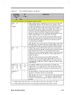
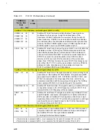
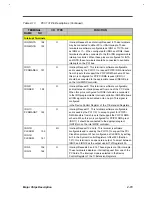
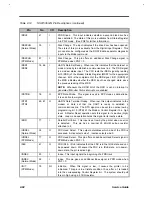
Table 2-13
PCI1131 Pin Descriptions (Continued)
TERMINAL
NAME NO
I /O
TYPE
FUNCTION
Interrupt Terminals
IRQ15/
RI_OUT 163
I/O
Interrupt Request 15. This terminal indicates an interrupt request
from one of the PC Cards. RI_OUT allows the RI input from the 1 6-
bit PC Card, CSTSCHG from CardBus Cards or PC Card removal
events to be output to the system. This signal is configured in the
Card Control Register of the TI Extension Registers.
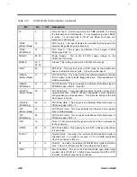
PC Card Power Switch Terminals
LATCH 150
O
Power Switch Latch is asserted by the PCI1131 to indicate to the PC
Card power switch that the data on the DATA line is valid.
CLOCK 151
O
Power Switch Clock. Information on the DATA line is sampled at the
rising edge of CLOCK. The frequency of the clock is derived from
dividing the PCICLK by 36. The maximum frequency of this signal is
2 MHz.
DATA
152
O
Power Switch Data is used by the PCI1131 to serially communicate
socket power control information.
Speaker Control Terminal
SPKROUT/
SUSPEND 149
I/O
Speaker. SPKROUT carries the digital audio signal from the PC
Card.
SUSPEND, when enabled, this signal places the PCI1131 in
PCI1131 Suspend Mode (Section 6.0) . This pin is configured in the
Card Control Register (Section 7.29) of the TI Extension Registers.
Power Supply Terminals
GND
13,22,44 75 96,129,
153, 167, 81
194,207
I
Device ground terminals
VccA
120
I
Power-supply terminal for PC Card A (5V or 3.3V)
VccB
38
I
Power-supply terminal for PC Card B (5V or 3.3 V)
VccP
148, 172
I
Power-supply terminal for PCI interface (5V or 3.3V)
Vcc
7, 31, 64, 86, 113,
143,164, 175, 187,
201
I
Power-Supply terminal for core logic (3.3V)
Содержание Extensa 61X
Страница 1: ...TI Extensa 61X Series AcerNote 370P Notebook Service Guide PART NO 2238309 0809 DOC NO PRINTED IN USA ...
Страница 6: ...vi ...
Страница 26: ...1 8 Service Guide Figure 1 5 Main Board Layout Bottom Side ...
Страница 49: ...System Introduction 1 31 1 5 1 3 Power Management Figure 1 14 Power Management Block Diagram ...
Страница 55: ...System Introduction 1 37 1 6 System Block Diagram Figure 1 15 System Block Diagram ...
Страница 64: ...Major Chips Description 2 7 2 2 5 Pin Diagram Figure 2 4 M1521 Pin Diagram ...
Страница 99: ...2 42 Service Guide 2 5 3 Pin Diagram Figure 2 10 C T 65550 Pin Diagram ...
Страница 116: ...Major Chips Description 2 59 2 6 4 Block Diagram Figure 2 11 Functional Block Diagram 16 bit PC Card Interface ...
Страница 117: ...2 60 Service Guide Figure 2 12 Functional block diagram CardBus Card Interface ...
Страница 118: ...Major Chips Description 2 61 2 6 5 Pin Diagram Figure 2 13 PCI to PC Card 16 bit terminal assignments ...
Страница 119: ...2 62 Service Guide Figure 2 14 PCI to CardBus terminal assignments ...
Страница 135: ...2 78 Service Guide 2 7 3 Pin Diagram Figure 2 16 NS87336VJG Pin Diagram ...
Страница 145: ...2 88 Service Guide 2 8 2 Pin Diagram Figure 2 17 YMF715 Block Diagram ...
Страница 185: ...Disassembly and Unit Replacement 4 5 Figure 4 3 Disassembly Sequence Flowchart ...
Страница 209: ...B 2 Service Guide ...
Страница 210: ...Exploded View Diagram B 3 ...
Страница 217: ...A p p e n d i x D A p p e n d i x D Schematics This appendix shows the schematic diagrams of the notebook ...


