Major Chips Description
2-3
•
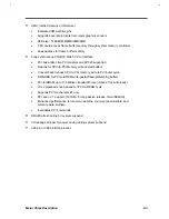
UMA (unified memory architecture)
•
Dedicated UMA arbiter pins
•
Supports several protocols from major graphics vendors
•
SFB size : 512KB/1MB/2MB/3MB/4MB
•
CPU could access frame buffer memory through system memory controller
•
Alias address for frame buffer memory
•
Fully synchronous 25/30/33 MHz 5V PCI interface
•
PCI bus arbiter: five PCI masters and M1523 supported
•
Dwords for CPU-to-PCI Memory write posted buffers
•
Convert back-to-back CPU to PCI memory write to PCI burst cycle
•
DWORDS for PCI-to-DRAM write-posted/read-prefetching buffers
•
PCI-to-DRAM up to 133 MB/sec bandwidth (even when L1/L2 write-back)
•
L1/L2 pipelined snoop ahead for PCI-to-DRAM cycle
•
Supports PCI mechanism #1 only
•
PCI spec. 2.1 support. [N(16/8)+8 rule, passive release, fair arbitration]
•
Enhanced performance for memory-read-line, memory-read-multiple, and
memory-write-multiple
•
Invalidates PCI commands
•
DRAM refresh during 5V system suspend
•
I/O leakage stopper for power saving during system suspend
•
328-pin or 388-pin BGA process
Содержание Extensa 61X
Страница 1: ...TI Extensa 61X Series AcerNote 370P Notebook Service Guide PART NO 2238309 0809 DOC NO PRINTED IN USA ...
Страница 6: ...vi ...
Страница 26: ...1 8 Service Guide Figure 1 5 Main Board Layout Bottom Side ...
Страница 49: ...System Introduction 1 31 1 5 1 3 Power Management Figure 1 14 Power Management Block Diagram ...
Страница 55: ...System Introduction 1 37 1 6 System Block Diagram Figure 1 15 System Block Diagram ...
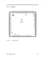
Страница 64: ...Major Chips Description 2 7 2 2 5 Pin Diagram Figure 2 4 M1521 Pin Diagram ...
Страница 99: ...2 42 Service Guide 2 5 3 Pin Diagram Figure 2 10 C T 65550 Pin Diagram ...
Страница 116: ...Major Chips Description 2 59 2 6 4 Block Diagram Figure 2 11 Functional Block Diagram 16 bit PC Card Interface ...
Страница 117: ...2 60 Service Guide Figure 2 12 Functional block diagram CardBus Card Interface ...
Страница 118: ...Major Chips Description 2 61 2 6 5 Pin Diagram Figure 2 13 PCI to PC Card 16 bit terminal assignments ...
Страница 119: ...2 62 Service Guide Figure 2 14 PCI to CardBus terminal assignments ...
Страница 135: ...2 78 Service Guide 2 7 3 Pin Diagram Figure 2 16 NS87336VJG Pin Diagram ...
Страница 145: ...2 88 Service Guide 2 8 2 Pin Diagram Figure 2 17 YMF715 Block Diagram ...
Страница 185: ...Disassembly and Unit Replacement 4 5 Figure 4 3 Disassembly Sequence Flowchart ...
Страница 209: ...B 2 Service Guide ...
Страница 210: ...Exploded View Diagram B 3 ...
Страница 217: ...A p p e n d i x D A p p e n d i x D Schematics This appendix shows the schematic diagrams of the notebook ...

