Major Chips Description
2-33
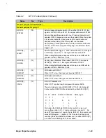
Table 2-4
M7101 Pin Descriptions (Continued)
Name
No.
Type
Description
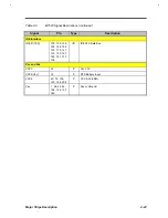
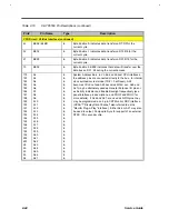
General purpose I/O interface(24)
General purpose I/O group C
GPIOC5
/EXTSW
(78)
External suspend/resume switch. When offset 0F6h D10=0, this
signal is GPIOC5. When D10=1, this signal will become EXTSW.
External Suspend/Resume switch input. Pressing this switch will
generate SMIJ to suspend or resume the system. When the system
is at resume status(On, Doze), pressing this switch will enter
Suspend status(Sleep). When the system is at Suspend
status(Sleep), pressing the switch will enter ON status. Debounce
circuit is built in. Both rising and falling edge are detected. Smith-
trigger input.
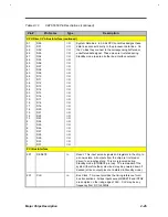
GPIOC[4]
/EJECT
(77)
External Eject SMIJ trigger. 1. When index 0F6h D7=0, this signal
is GPIOC(4). When it is 1, this signal will become EJECT
When a rising/falling edge happens at this input, an SMIJ will be
generated. Built in debounce circuit.
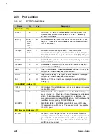
GPIOC[3]
/DOCKJ
(75)
Docking insert detected. When index 0F6h D7=0, this signal is
GPIOC[3]. When it is 1, this signal will become DOCKJ
When a rising/falling edge happens at this input, an SMIJ will be
generated. Built in debounce circuit.
GPIOC[2]
/BIOSA17
(74)
BIOS address ROM A17
When CCFT is low, this signal will become BIOSA17.
GPIOC[1]
/BIOSA16
(73)
BIOS address ROM A16
When CCFT is low, this signal will become BIOSA16.
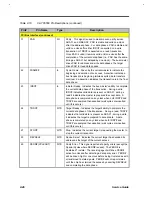
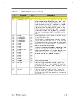
GPIOC[0]
/ISA16
(72)
ISA SLOT address A16
When CCFT is pulled low, this signal will become ISA16.
These two signals connect BIOS ROM A17 & A16 to distinguish
the four parts of BIOS ROM and decided by offset 0D2h D[2:1].
D2 D1 ISA16 BIOSA17 BIOSA16 ROM region
X X 1 0 1 1
X 0 0 0 0 0
0 1 0 1 0 2
1 1 0 1 1 3
We divided the 256K byte ROM into four parts. E region will
occupy three parts--0,2,3, F region will occupy one part--1. So,
when CPU accesses to F region, that is, ISA16=1, then system will
access ROM region 1, F segment. The E region has three parts
overlaying the same address, software can use offset 0D2h D[2:1]
to choose which ROM region to be accessed.
Содержание Extensa 61X
Страница 1: ...TI Extensa 61X Series AcerNote 370P Notebook Service Guide PART NO 2238309 0809 DOC NO PRINTED IN USA ...
Страница 6: ...vi ...
Страница 26: ...1 8 Service Guide Figure 1 5 Main Board Layout Bottom Side ...
Страница 49: ...System Introduction 1 31 1 5 1 3 Power Management Figure 1 14 Power Management Block Diagram ...
Страница 55: ...System Introduction 1 37 1 6 System Block Diagram Figure 1 15 System Block Diagram ...
Страница 64: ...Major Chips Description 2 7 2 2 5 Pin Diagram Figure 2 4 M1521 Pin Diagram ...
Страница 99: ...2 42 Service Guide 2 5 3 Pin Diagram Figure 2 10 C T 65550 Pin Diagram ...
Страница 116: ...Major Chips Description 2 59 2 6 4 Block Diagram Figure 2 11 Functional Block Diagram 16 bit PC Card Interface ...
Страница 117: ...2 60 Service Guide Figure 2 12 Functional block diagram CardBus Card Interface ...
Страница 118: ...Major Chips Description 2 61 2 6 5 Pin Diagram Figure 2 13 PCI to PC Card 16 bit terminal assignments ...
Страница 119: ...2 62 Service Guide Figure 2 14 PCI to CardBus terminal assignments ...
Страница 135: ...2 78 Service Guide 2 7 3 Pin Diagram Figure 2 16 NS87336VJG Pin Diagram ...
Страница 145: ...2 88 Service Guide 2 8 2 Pin Diagram Figure 2 17 YMF715 Block Diagram ...
Страница 185: ...Disassembly and Unit Replacement 4 5 Figure 4 3 Disassembly Sequence Flowchart ...
Страница 209: ...B 2 Service Guide ...
Страница 210: ...Exploded View Diagram B 3 ...
Страница 217: ...A p p e n d i x D A p p e n d i x D Schematics This appendix shows the schematic diagrams of the notebook ...


