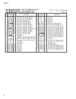
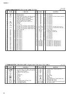
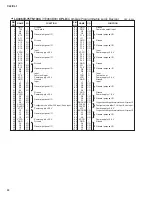
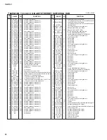
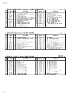


CL3/CL1
90
PIN
NO.
I/O
FUNCTION
NAME
PIN
NO.
I/O
FUNCTION
NAME
KSZ8051RNL
(YD367B00)
PHY
CPU: IC402
1
2
3
4
5
6
7
8
9
10
11
12
13
14
15
16
17
18
GND
VDD_1.2
VDDA_3.3
RXM
RXP
TXM
TXP
XO
XI
REXT
MDIO
MDC
RXD3/
PHYAD0
RXD2/
PHYAD1
RXD1/
PHYAD2
RXD0/
DUPLEX
VDDIO
RXDV/
CONFIG2
-
-
-
I/O
I/O
I/O
I/O
O
I
I
I/O
I
I/O
I/O
I/O
I/O
-
I/O
Ground
1.2V core V
DD
3.3V analog V
DD
Physical receive or transmit signal (- differential)
Physical receive or transmit signal (+ differential)
Physical transmit or receive signal (- differential)
Physical transmit or receive signal (+ differential)
Crystal feedback – for 25 MHz crystal
Crystal / Oscillator / External Clock Input
Set physical transmit output current
Management Interface (MII) Data I/O
Management Interface (MII) Clock Input
MII Mode: MII Receive Data Output[3]/
Config Mode: The pull-up/pull-down value is latched
as PHYADDR[0] at the de-assertion of reset
MII Mode: MII Receive Data Output[2]/
Config Mode: The pull-up/pull-down value is latched
as PHYADDR[1] at the de-assertion of reset
MII Mode: MII Receive Data Output[1]/
Config Mode: The pull-up/pull-down value is latched
as PHYADDR[2] at the de-assertion of reset
MII Mode: MII Receive Data Output[0]/
Config Mode: The pull-up/pull-down value is latched
as DUPLEX at the de-assertion of reset
3.3V, 2.5V or 1.8V digital V
DD
MII Mode: MII Receive Data Valid Output/
Config Mode: The pull-up/pull-down value is latched
as CONFIG2 at the de-assertion of reset
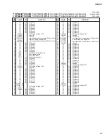
19
20
21
22
23
24
25
26
27
28
29
30
31
32
RXC/
B-CAST_OFF
RXER/
ISO
INTRP/
NAND_Tree#
TXC
TXEN
TXD0
TXD1
TXD2
TXD3
COL/
CONFIG0
CRS/
CONFIG1
LED0/
NWAYEN
LED1/
SPEED
RST#
GND
I/O
I/O
I/O
I/O
I
I
I
I
I
I/O
I/O
I/O
I/O
I/O
-
MII Mode: MII Receive Clock Output/
Config Mode: The pull-up/pull-down value is latched
as B-CAST_OFF at the de-assertion of reset
MII Mode: MII Receive Error Output/
Config Mode: The pull-up/pull-down value is latched
as ISOLATE at the de-assertion of reset
Interrupt Output: Programmable Interrupt Output
Config Mode: The pull-up/pull-down value is latched
as NAND Tree# at the de-assertion of reset.
MII Mode: MII Transmit Clock Output
MII Back-to-Back Mode: MII Transmit Clock Input
MII Mode: MII Transmit Enable Input
MII Mode: MII Transmit Data Input[0]
MII Mode: MII Transmit Data Input[1]
MII Mode: MII Transmit Data Input[2]
MII Mode: MII Transmit Data Input[3]
MII Mode: MII Collision Detect Output /
Config Mode: The pull-up/pull-down value is latched
as CONFIG0 at the de-assertion of reset
MII Mode: MII Carrier Sense Output /
Config Mode: The pull-up/pull-down value is latched
as CONFIG1 at the de-assertion of reset
LED Output: Programmable LED0 Output /
Config Mode: Latched as Auto-Negotiation Enable
(register 0h, bit 12) at the de-assertion of reset
LED Output: Programmable LED1 Output /
Config Mode: Latched as SPEED (register 0h, bit
13) at the de-assertion of reset
Chip Reset (active low)
Ground
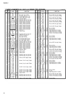
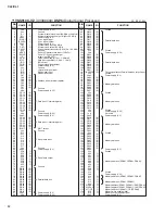
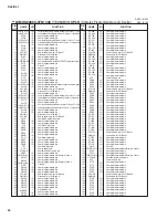
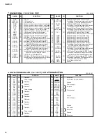
PADDLE
PIN
NO.
I/O
FUNCTION
NAME
PIN
NO.
I/O
FUNCTION
NAME
'
9
&&
'
'
*1'
'
'
9
&&
'
'
*1'
'
'
1&
'
'
*1'
'
'
'
9
&&
'
'
*1'
,2
,2
,2
,2
,2
,2
,2
,2
,2
,2
,2
,2
,2
,2
,2
,2
'DWDEXV
3RZHUVXSSO\
'DWDEXV
*URXQG
'DWDEXV
3RZHUVXSSO\
'DWDEXV
*URXQG
'DWDEXV
1RWXVHG
'DWDEXV
*URXQG
'DWDEXV
3RZHUVXSSO\
'DWDEXV
*URXQG
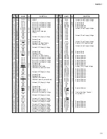
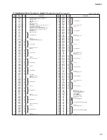
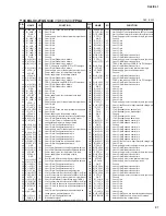
'
&/.,1
6+7'1
3//*1'
3//9
&&
3//*1'
/9'6*1'
&/.2873
&/.2870
<3
<0
/9'6*1'
/9'69
&&
<3
<0
<3
<0
/9'6*1'
1&
'
'
*1'
'
'
,2
,
2
2
,2
,2
,2
,2
'DWDEXV
,QSXWFORFNIRU&/.,10,',
*URXQG
3RZHUVXSSO\
*RURXQG
&ORFNRXWSXW
*URXQG
3RZHUVXSSO\
*URXQG
1RWXVHG
'DWDEXV
*URXQG
'DWDEXV
&38,&
SN75LVDS84ADGGR
;$5
LVDS TRANSMITTER
Summary of Contents for CL3
Page 7: ...7 CL3 CL1 DIMENSIONS CL3 CL1 648 15 201 130 299 667 839 15 201 130 299 667 Unit mm...
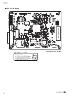
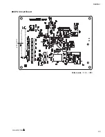
Page 95: ...95 CL3 CL1 CPU Circuit Board Pattern side to DSP CN101 2NA WY67750 1...
Page 101: ...101 CL3 CL1 DNTU Circuit Board Pattern side Scale 80 100 2NA WZ20390 5...
Page 102: ...CL3 CL1 102 2NA WY63530 FX Circuit Board WR 63 1 Component side Scale 95 100...
Page 103: ...103 CL3 CL1 2NA WY63530 FX Circuit Board Pattern side Scale 95 100...
Page 105: ...105 CL3 CL1 HAAD Circuit Board Pattern side Scale 90 100 2NA WY64340 2...
Page 107: ...107 CL3 CL1 2NA WY63490 Component side JK Circuit Board WR 63 1...
Page 109: ...109 CL3 CL1 Component side TBPHN Circuit Board WR 06 1 WR 63 1 2NA WY64360 1...
Page 110: ...CL3 CL1 110 Component side PN8 Circuit Board to FD8 CN902 or FD8CN CN902 2NA WY53120 2...
Page 118: ...CL3 CL1 118 Component side PNENL Circuit Board to PN8 CN001 2NA WY53130 1...
Page 160: ...CL3 CL1 160 1 18 LCD Test LCD LCD 1 3 2 9 5 OK NG 1 2 H 3 O X O 4 BOX 5x4...
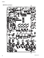
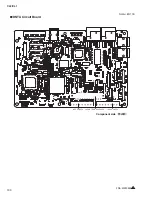
Page 382: ...7 MBCL CIRCUIT BOARDS A A A A 2NA WY53200 1 MB Circuit Board Component side...
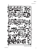
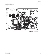
Page 383: ...MBCL 8 MB Circuit Board DSUB PH CONNECTOR ASSEMBLY B B B B 2NA WY53200 1 Pattern side...


