


CL3/CL1
141
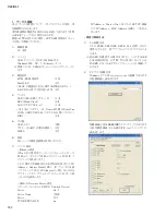
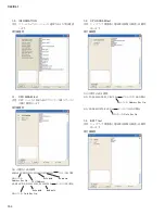
1-9. SLOT
Test
Contents: Checks the power voltage supplied to each interface and SLOT of MY SLOT.
3SLOT check
Example of executing screen
Total judgment slot by slot
Number of the slot
being checked
Only SLOT 1 is valid
Test required/not required
Number of SIO in SLOT
Data being
transmitted/received are
indicated.
The check result is NG
because the numeric
value is different.
The right end shows
LSB, indicating the bit of
0=OK, X=NG.
Judgment box when POWER = MANUAL is used.
Checking SLOT power voltage
Take measurement at each terminal of MY16-EX check jig using
a tester in the Manual mode for judgment.(For measurement,
connect a cable to the connector CN102 of EX.)
The COM test is applicable to SLOT1 only.
1-10. AIN/AOUT Test
This testing function is unused.
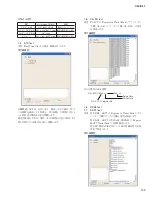
1-11. WORD CLOCK Test
Contents: Checks WORD CLOCK OUT
→
IN automatically
by counting it at PLLPU.
(Fs=44.1/48 kHz) Checks PLL LOCK by reading
the UNLOCK signal when the clock has been
stabilized after the Fs change (after about 200 ms).
Example of executing screen
Various Fs (frequencies) for the PLL LOCK check are
generated in Internal Clock of FPGA.
Fs = 44.1 kHz, 48 kHz
Summary of Contents for CL3
Page 7: ...7 CL3 CL1 DIMENSIONS CL3 CL1 648 15 201 130 299 667 839 15 201 130 299 667 Unit mm...
Page 95: ...95 CL3 CL1 CPU Circuit Board Pattern side to DSP CN101 2NA WY67750 1...
Page 101: ...101 CL3 CL1 DNTU Circuit Board Pattern side Scale 80 100 2NA WZ20390 5...
Page 102: ...CL3 CL1 102 2NA WY63530 FX Circuit Board WR 63 1 Component side Scale 95 100...
Page 103: ...103 CL3 CL1 2NA WY63530 FX Circuit Board Pattern side Scale 95 100...
Page 105: ...105 CL3 CL1 HAAD Circuit Board Pattern side Scale 90 100 2NA WY64340 2...
Page 107: ...107 CL3 CL1 2NA WY63490 Component side JK Circuit Board WR 63 1...
Page 109: ...109 CL3 CL1 Component side TBPHN Circuit Board WR 06 1 WR 63 1 2NA WY64360 1...
Page 110: ...CL3 CL1 110 Component side PN8 Circuit Board to FD8 CN902 or FD8CN CN902 2NA WY53120 2...
Page 118: ...CL3 CL1 118 Component side PNENL Circuit Board to PN8 CN001 2NA WY53130 1...
Page 160: ...CL3 CL1 160 1 18 LCD Test LCD LCD 1 3 2 9 5 OK NG 1 2 H 3 O X O 4 BOX 5x4...
Page 382: ...7 MBCL CIRCUIT BOARDS A A A A 2NA WY53200 1 MB Circuit Board Component side...
Page 383: ...MBCL 8 MB Circuit Board DSUB PH CONNECTOR ASSEMBLY B B B B 2NA WY53200 1 Pattern side...