


CL3/CL1
127
1. 準備
1-1. 測定器
検査に使用する測定器は、各検査項目を十分精度良く測定
できる精度及び確度をもつものを使用してください。
測定器の入力インピーダンスは 100 k Ω以上とします。
• System Two
• テスター
• フィルター(12.7 kHz、‒6 dB/OCT)
• レベル計
1-2. 条件
◇ 特に指定しないときは以下の条件とします。
• WORD CLOCK は INT48 kHz にします。
• +48 V MASTER を ON にします。
• 測定 CH のみ ON とします。
PAN :
センター
GAIN :
MIN
FADER :
NOMINAL(0 dB)
PHONES LEVEL :
MAX
TALKBACK GAIN :
MAX
• 0 dBu = 0.775 Vrms
• 0 dBFS = 0 デシベル・フルスケール
• 発振器の出力インピーダンスは 150 Ωとします。
• ノイズ測定は 12.7 kHz、‒6 dB/OCT の LPF で補正
します。
(実効値ではなく平均値での測定とします。)
• 歪み測定は 80 kHz、‒18 dB/OCTのLPF で補正します。
◇ アナログ出力の検査時は以下の条件を追加、変更します。
• 最大出力測定時、特に指定のない場合は内蔵オシレー
ターから 0 dB を出力します。
• アナログ出力の負荷は、
OMNI OUT :
600 Ω
PHONES :
8 Ω
とします。
1-3. プログラムのアップデート
本体のプログラムが最新バージョンになっていない場合、最
新のプログラムにバージョンアップする必要があります。
※ 最新のプログラムは、YSISS ホームページよりダウンロードして、
USB 記憶装置に保存します。
(1) 本体のプログラムのバージョン確認方法
LCD 画面内で
[SET UP]
を押すと、 SETUP
のページ
画面に現在のバージョンが表示されます。
(2) プログラムのアップデート方法
プログラムのアップデート方法は、
「FIRMWARE のアップ
デート」の項を参照してください。
(165 ページ)
1-4. 初期化
[STORE]
ス イッ チ を 押 し な が ら 電 源 を 立 ち 上 げ、
INITIALIZE ALL MEMORIES
を実行して、初期化
を行います。
(167 ページ)
1-5. フェーダーのキャリブレーション
フェーダー の キャリブ レ ーションの 方 法 は、
「FADER
CALIBRATION」の項を参照してください。
(171 ページ)
1-6. カラーバーのキャリブレーション
カラーバーのキャリブレーションの方法は、
「カラーバーと
CH NAME LCD のキャリブレーション」の項を参照してく
ださい。
(173 ページ)
1-7. CPU シートの MRAM のバックアップ検査
電 源を ON にした 時、LCD の 画 面 に、 Memory Error!
Current Memories were Initialized. が表示されないこと
を確認します。
2. ANALOG IN / OUT 特性検査
2-1. OMNI IN 1-8 → OMNI OUT 1-8
条件 CH1‒8 の INPUT (XLR) からアナログ信号を入力
し、CH1‒8 出力から出力される信号を計測します。
OMNI IN CH1‒8 を OMNI OUT 1‒8 にアサインし
ます。
A. AIN MAIN
1
利得
入力周波数
入力レベル
規定出力レベル
許容範囲
1 kHz
+10 dBu
+4 dBu
+4 ± 2 dBu
2
歪率
入力周波数
出力レベル
許容範囲
1 kHz
+22 dBu
0.01 %以下
3
ノイズレベル
条件 測定する CH IN を 150 Ωでショートします。
許容範囲
‒80 dBu 以下
4
残留ノイズ(OMNI OUT 1‒8)
条件 OMNI IN CH1‒8 を OFF にします。
許容範囲
‒88 dBu 以下
5
CH1‒8 間のレベル差
①で測定した利得差の範囲を以下の様になることを確認
します。
許容範囲
1 dB 以内
検査
Summary of Contents for CL3
Page 7: ...7 CL3 CL1 DIMENSIONS CL3 CL1 648 15 201 130 299 667 839 15 201 130 299 667 Unit mm...
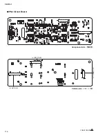
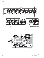
Page 95: ...95 CL3 CL1 CPU Circuit Board Pattern side to DSP CN101 2NA WY67750 1...
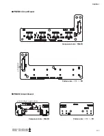
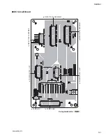
Page 101: ...101 CL3 CL1 DNTU Circuit Board Pattern side Scale 80 100 2NA WZ20390 5...
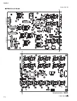
Page 102: ...CL3 CL1 102 2NA WY63530 FX Circuit Board WR 63 1 Component side Scale 95 100...
Page 103: ...103 CL3 CL1 2NA WY63530 FX Circuit Board Pattern side Scale 95 100...
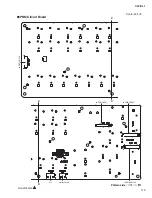
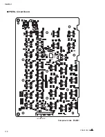
Page 105: ...105 CL3 CL1 HAAD Circuit Board Pattern side Scale 90 100 2NA WY64340 2...
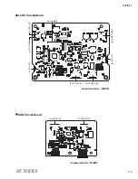
Page 107: ...107 CL3 CL1 2NA WY63490 Component side JK Circuit Board WR 63 1...
Page 109: ...109 CL3 CL1 Component side TBPHN Circuit Board WR 06 1 WR 63 1 2NA WY64360 1...
Page 110: ...CL3 CL1 110 Component side PN8 Circuit Board to FD8 CN902 or FD8CN CN902 2NA WY53120 2...
Page 118: ...CL3 CL1 118 Component side PNENL Circuit Board to PN8 CN001 2NA WY53130 1...
Page 160: ...CL3 CL1 160 1 18 LCD Test LCD LCD 1 3 2 9 5 OK NG 1 2 H 3 O X O 4 BOX 5x4...
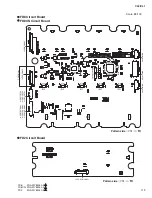
Page 382: ...7 MBCL CIRCUIT BOARDS A A A A 2NA WY53200 1 MB Circuit Board Component side...
Page 383: ...MBCL 8 MB Circuit Board DSUB PH CONNECTOR ASSEMBLY B B B B 2NA WY53200 1 Pattern side...