
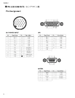
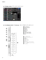


5
CL3/CL1
(入出力仕様)
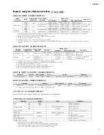
Input/output characteristics
ANALOG INPUT CHARACTERISTICS
*1. Sensitivity is the lowest level that will produce an output of +4dBu (1.23V) or the nominal output level when the unit is set to maximum
gain. (all faders and level controls are maximum position.)
*2. XLR-3-31 type connectors are balanced. (1= GND, 2= HOT, 3= COLD)
*3. In these specifications, 0dBu= 0.775 Vrms.
*4. All input AD converters are 24bit linear, 128times oversampling.
*5. +48V DC ( phantom power ) is supplied to OMNI IN (1-8) and TALKBACK XLR type connectors via each individual software controlled
switches.
ANALOG OUTPUT CHARACTERISTICS
*1. XLR-3-32 type connectors are balanced. (1= GND, 2= HOT, 3= COLD)
*2. PHONES stereo phone jack is unbalanced. (Tip= LEFT, Ring= RIGHT, Sleeve= GND)
*3. In these specifications, 0dBu= 0.775 Vrms.
*4. All output DA converters are 24bit, 128times oversampling.
*5. There are switches inside the body to preset the maximum output level.
*6. The position of the level control is 10dB lowered from Max.
DIGITAL INPUT & OUTPUT CHARACTERISTICS
DIGITAL OUTPUT CHARACTERISTICS
*1. XLR-3-32 type connectors are balanced. (1= GND, 2= HOT, 3= COLD)
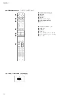
I/O SLOT (1-3) CHARACTERISTICS
Each I/O Slot accepts a mini-YGDAI card. Only Slot1 has a serial interface.
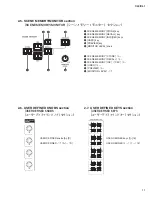
CONTROL I/O CHARACTERISTICS
*1. Input pin: TTL level, w/ internal pull-up (47k
Ω
)
Output pin: Open drain output (Vmax=12V,
maximum sink current/pin=75mA)
Power supply pin: Output voltage
Vp=5V, Max. output current Imax=300mA
*2. 4pin= +12V, 3pin= GND, Lamp rating 5W. Voltage control by software.
Input
Terminals
GAIN
Actual Load
Impedance
For Use With
Nominal
Input Level
Connector
Sensitivity
*1
Nominal
Max. before clip
OMNI IN 1-8
+66dB
10k
Ω
50-600
Ω
Mics
& 600
Ω
Lines
–82dBu (61.6μV)
–62dBu (0.616mV)
–42dBu (6.16mV)
XLR-3-31 type
(Balanced)
*2
+18dB
–34dBu (15.5mV)
–14dBu (155mV)
+6dBu (1.55V)
+17dB
3k
Ω
–33dBu (17.4mV)
–13dBu (174mV)
+7dBu (1.74V)
–6dB
–10dBu (245mV)
+10dBu (2.45V)
+30dBu (24.5V)
TALKBACK
+64dB
10k
Ω
50-600
Ω
Mics
& 600
Ω
Lines
–70dBu (0.245mV) –60dBu (0.775mV)
–40dBu (7.75mV)
XLR-3-31 type
(Balanced)
*2
+20dB
–26dBu (38.8mV)
–16dBu (0.123V)
+4dBu (1.23V)
Output
Terminals
Actual Source
Impedance
For Use With
Nominal
GAIN SW
*5
Output Level
Connector
Nominal
Max. before clip
OMNI OUT 1-8
+24dB (default)
+4dBu (1.23V)
+24dBu (12.3V)
XLR-3-32 type
(Balanced)
*1
+18dB
–2dBu (616mV)
+18dBu (6.16V)
PHONES
15
Ω
8
Ω
Phones
–
75mW
*6
150mW
Stereo Phone Jack (TRS)
(Unbalanced)
*2
40
Ω
Phones
–
65mW
*6
150mW
r
o
t
c
e
n
n
o
C
o
i
d
u
A
l
e
v
e
L
h
t
g
n
e
l
a
t
a
D
t
a
m
r
o
F
l
a
n
i
m
r
e
T
Primary/Secondary
Dante
24bit or 32bit
1000Base-T
64ch Input/64ch Output @48kHz
etherCON Cat5e
r
o
t
c
e
n
n
o
C
l
e
v
e
L
h
t
g
n
e
L
a
t
a
D
t
a
m
r
o
F
l
a
n
i
m
r
e
T
DIGITAL OUT
AES/EBU
AES/EBU Professional Use
24bit
RS422
XLR-3-32 type (Balanced)
*1
Terminal
Format
Level
Connector
MIDI
IN
MIDI
–
DIN Connector 5P
OUT
MIDI
–
DIN Connector 5P
WORD CLOCK
IN
–
TTL/75
Ω
terminated
BNC Connector
OUT
–
TTL/75
Ω
BNC Connector
GPI (5IN/5OUT)
–
–
D Sub Connector 15P (Female)
*1
NETWORK
IEEE802.3
10BASE-T/100Base-TX
RJ-45
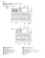
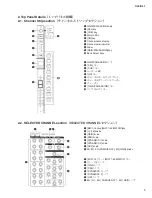
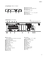
LAMP (CL5: x3, CL3: x2, CL1: x1)
–
0V-12V
*4
XLR-4-31 type
*2
USB HOST
USB 2.0
–
USB A Connector (Female)
DC POWER INPUT
–
–
JL05 Connector
METER (CL3/CL1 only)
–
–
D Sub Connector 9P (Female)
75
Ω
600
Ω
Lines
Summary of Contents for CL3
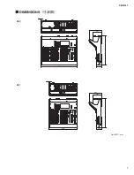
Page 7: ...7 CL3 CL1 DIMENSIONS CL3 CL1 648 15 201 130 299 667 839 15 201 130 299 667 Unit mm...
Page 95: ...95 CL3 CL1 CPU Circuit Board Pattern side to DSP CN101 2NA WY67750 1...
Page 101: ...101 CL3 CL1 DNTU Circuit Board Pattern side Scale 80 100 2NA WZ20390 5...
Page 102: ...CL3 CL1 102 2NA WY63530 FX Circuit Board WR 63 1 Component side Scale 95 100...
Page 103: ...103 CL3 CL1 2NA WY63530 FX Circuit Board Pattern side Scale 95 100...
Page 105: ...105 CL3 CL1 HAAD Circuit Board Pattern side Scale 90 100 2NA WY64340 2...
Page 107: ...107 CL3 CL1 2NA WY63490 Component side JK Circuit Board WR 63 1...
Page 109: ...109 CL3 CL1 Component side TBPHN Circuit Board WR 06 1 WR 63 1 2NA WY64360 1...
Page 110: ...CL3 CL1 110 Component side PN8 Circuit Board to FD8 CN902 or FD8CN CN902 2NA WY53120 2...
Page 118: ...CL3 CL1 118 Component side PNENL Circuit Board to PN8 CN001 2NA WY53130 1...
Page 160: ...CL3 CL1 160 1 18 LCD Test LCD LCD 1 3 2 9 5 OK NG 1 2 H 3 O X O 4 BOX 5x4...
Page 382: ...7 MBCL CIRCUIT BOARDS A A A A 2NA WY53200 1 MB Circuit Board Component side...
Page 383: ...MBCL 8 MB Circuit Board DSUB PH CONNECTOR ASSEMBLY B B B B 2NA WY53200 1 Pattern side...


