


CL3/CL1
56
28CC1-2001089251-1
4
not installed
not installed
not installed
not installed
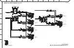
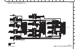
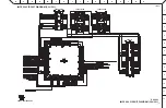
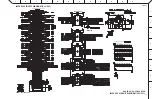
OP AMP
OP AMP
OP AMP
OP AMP
OP AMP
OP AMP
OP AMP
OP AMP
OP AMP
ADC
ADC
OP AMP
OP AMP
OP AMP
MULTIPLEXER
MULTIPLEXER
MULTIPLEXER
MULTIPLEXER
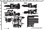
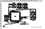
GAIN SETTING CHART
Rated Input
(dB)
(定格入力)
ANALOG INPUT CHARACTERISTICS
Input
Terminals
GAIN
Actual Load
Impedance
For Use With
Nominal
Input Level
Connector
Sensitivity
*1
Nominal
OMNI IN 1-8
+66dB
10k
1
50-600
1
Mics
& 600
1
Lines
–82dBu (61.6μV)
–62dBu (0.616mV)
–42dBu (6.16mV)
XLR-3-31 type
(Balanced)
*2
+18dB
–34dBu (15.5mV)
–14dBu (155mV)
+6dBu (1.55V)
+17dB
3k
1
–33dBu (17.4mV)
–13dBu (174mV)
+7dBu (1.74V)
–6dB
–10dBu (245mV)
+10dBu (2.45V)
+30dBu (24.5V)
TALKBACK
+64dB
10k
1
50-600
1
Mics
& 600
1
Lines
–70dBu (0.245mV) –60dBu (0.775mV)
–40dBu (7.75mV)
XLR-3-31 type
(Balanced)
*2
+20dB
–26dBu (38.8mV)
–16dBu (0.123V)
+4dBu (1.23V)
Max. before clip
*1. Sensitivity is the lowest level that will produce an output of +4dBu (1.23V) or the nominal output level when the unit is set to maximum gain.
(all faders and level controls are maximum position.)
*2. XLR-3-31 type connectors are balanced. (1= GND, 2= HOT, 3= COLD)
*3. In these specifications, 0dBu= 0.775 Vrms.
*4. All input AD converters are 24bit linear, 128times oversampling.
*5. +48V DC ( phantom power ) is supplied to OMNI IN (1-8) and TALKBACK XLR type connectors via each individual software controlled switches.
A
B
C
D
E
F
G
H
I
J
K
L
M
N
O
P
Q
R
S
T
U
V
W
1
2
3
4
5
6
7
8
9
10
11
12
13
14
15
16
17
■
HAAD 001 CIRCUIT DIAGRAM (CL3/CL1)
■
HAAD 001 CIRCUIT DIAGRAM (CL3/CL1)
HEAD AMP AND AD CONVERTER
Summary of Contents for CL3
Page 7: ...7 CL3 CL1 DIMENSIONS CL3 CL1 648 15 201 130 299 667 839 15 201 130 299 667 Unit mm...
Page 95: ...95 CL3 CL1 CPU Circuit Board Pattern side to DSP CN101 2NA WY67750 1...
Page 101: ...101 CL3 CL1 DNTU Circuit Board Pattern side Scale 80 100 2NA WZ20390 5...
Page 102: ...CL3 CL1 102 2NA WY63530 FX Circuit Board WR 63 1 Component side Scale 95 100...
Page 103: ...103 CL3 CL1 2NA WY63530 FX Circuit Board Pattern side Scale 95 100...
Page 105: ...105 CL3 CL1 HAAD Circuit Board Pattern side Scale 90 100 2NA WY64340 2...
Page 107: ...107 CL3 CL1 2NA WY63490 Component side JK Circuit Board WR 63 1...
Page 109: ...109 CL3 CL1 Component side TBPHN Circuit Board WR 06 1 WR 63 1 2NA WY64360 1...
Page 110: ...CL3 CL1 110 Component side PN8 Circuit Board to FD8 CN902 or FD8CN CN902 2NA WY53120 2...
Page 118: ...CL3 CL1 118 Component side PNENL Circuit Board to PN8 CN001 2NA WY53130 1...
Page 160: ...CL3 CL1 160 1 18 LCD Test LCD LCD 1 3 2 9 5 OK NG 1 2 H 3 O X O 4 BOX 5x4...
Page 382: ...7 MBCL CIRCUIT BOARDS A A A A 2NA WY53200 1 MB Circuit Board Component side...
Page 383: ...MBCL 8 MB Circuit Board DSUB PH CONNECTOR ASSEMBLY B B B B 2NA WY53200 1 Pattern side...


