


CL3/CL1
123
6
Crosstalk between adjacent channels
Parameters: Turn on OMNI OUT of only one odd number
channel for output, turn off OMNI OUT of other
channels and measure the noise level of even
number channels next to the odd number channel
on both sides.
Short INPUT of the even number channels to be
measured with 150
Ω
.
Input Frequency
Output Level (Odd
Channel)
Permissible Range
(Even Channel)
1 kHz
+23 dBu
–57 dBu or below
Perform the same check on the even number channels.
7
Maximum output (OMNI OUT 1-8)
Parameters: Assign only the built-in oscillator to OMNI OUT
1-8.
Input
Frequency
Output Level
Permissible
Range
Permissible Range
(Distortion)
1 kHz
+24 dBu
+24±0.5 dBu
0.01 % or below
B. GAIN MAX
1
Gain (OMNI IN 1-8)
Input
Frequency
Input Level
Prescribed
Output Level
Permissible
Range
1 kHz
–62 dBu
+4 dBu
+4±2 dBu
2
Distortion (OMNI IN 1-8)
Input
Frequency
Output Level
Permissible
Range
1 kHz
+22 dBu
0.02 % or below
3
Noise level EIN (OMNI IN 1-8)
Parameters: Short CH IN to be measured with 150
Ω
.
Permissible Range
–62 dBu or below
If the measured value is out of the above permissible
range,con
fi
rm that “measured value – (Gain at 1kHz)
≦
-128”
is obtained.
4
Level difference (OMNI IN 1-8)
Con
fi
rm that the range of difference in the gain measured in
item
1
above is as follows.
Permissible Range
Within 2 dB
C. PHANTOM VOLTAGE (OMNI IN 1)
With No.2 and No.3 pins of XLR shorted and 10 k
Ω
load
connected between No.2 and No.1 pins, check that the voltage
is as follows when the +48 key is turned on.
Permissible Range
DC 33.6 – 36.1 V
Also, check that discharging starts immediately when the +48
key is turned off.
2-2. PHONES L, R
Parameters: Input from INPUT (XLR) of OMNI IN 1.
Assign OMNI IN 1 to STEREO.
Set MONITOR SOURCE to STEREO l/R.
Set PHONES LEVEL LINK to OFF.
1
Gain (PHONES L, R)
Input
Frequency
Input Level
Prescribed
Output Level
Permissible
Range
1 kHz
0 dBu
0 dBu
0±2 dBu
2
Distortion (PHONES L, R)
Input
Frequency
Output Level
Permissible
Range
1 kHz
0 dBu
0.15 or below
3
Residual noise (PHONES L, R)
Parameters: Turn off STEREO.
PHONES Level
Parameter Range
MAX
–79 dBu or below
MIN
–88 dBu or below
4
PHONES L to R level difference
Con
fi
rm that the range of difference in the gain measured in
item
1
above is as follows.
Permissible Range
Within 2 dB
5
Maximum output (PHONES L, R)
Parameters: Assign only the built-in oscillator to STEREO and
output -27 dB from the built-in oscillator.
Input
Frequency
Output Level
Permissible
Range
Permissible range
(Distortion)
1 kHz
+3 dBu
+3±0.5 dBu
0.15 % or below
6
L to R crosstalk
Parameters: Set PAN fully to the L side.
Input
Frequency
Output Level
Permissible
Range
1 kHz
+3 dBu
–56 dBu or blow
Perform the same check on the R side.
2-3. TALKBACK
Parameters: Use OMNI OUT 1 for the inspection.
Assign TALKBACK to MIX1.
Turn TALKBACK to ON.
A. GAIN MAX
1
Gain
Input
Frequency
Input Level
Prescribed
Output Level
Permissible
Range
1 kHz
–60 dBu
+4 dBu
+4±2 dBu
Summary of Contents for CL3
Page 7: ...7 CL3 CL1 DIMENSIONS CL3 CL1 648 15 201 130 299 667 839 15 201 130 299 667 Unit mm...
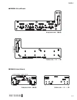
Page 95: ...95 CL3 CL1 CPU Circuit Board Pattern side to DSP CN101 2NA WY67750 1...
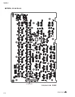
Page 101: ...101 CL3 CL1 DNTU Circuit Board Pattern side Scale 80 100 2NA WZ20390 5...
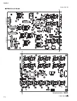
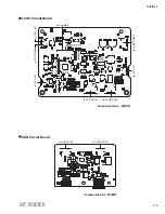
Page 102: ...CL3 CL1 102 2NA WY63530 FX Circuit Board WR 63 1 Component side Scale 95 100...
Page 103: ...103 CL3 CL1 2NA WY63530 FX Circuit Board Pattern side Scale 95 100...
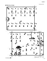
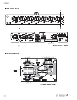
Page 105: ...105 CL3 CL1 HAAD Circuit Board Pattern side Scale 90 100 2NA WY64340 2...
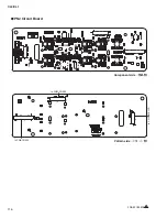
Page 107: ...107 CL3 CL1 2NA WY63490 Component side JK Circuit Board WR 63 1...
Page 109: ...109 CL3 CL1 Component side TBPHN Circuit Board WR 06 1 WR 63 1 2NA WY64360 1...
Page 110: ...CL3 CL1 110 Component side PN8 Circuit Board to FD8 CN902 or FD8CN CN902 2NA WY53120 2...
Page 118: ...CL3 CL1 118 Component side PNENL Circuit Board to PN8 CN001 2NA WY53130 1...
Page 160: ...CL3 CL1 160 1 18 LCD Test LCD LCD 1 3 2 9 5 OK NG 1 2 H 3 O X O 4 BOX 5x4...
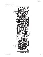
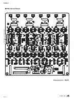
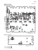
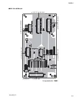
Page 382: ...7 MBCL CIRCUIT BOARDS A A A A 2NA WY53200 1 MB Circuit Board Component side...
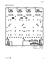
Page 383: ...MBCL 8 MB Circuit Board DSUB PH CONNECTOR ASSEMBLY B B B B 2NA WY53200 1 Pattern side...


