


CL3/CL1
148
●
CL3/CL1 テストプログラム
a. 本テストプログラムは CL3/CL1 の「サービス検査」に使用します。
検査は CL3/CL1 本体と PC に以下の表にある最新プログラムをロードしてから行ってください。
アップデートの方法は、165 ページの「FIRMWARE のアップデート」の項を参照してください。
※ テストプログラムは、YSISS ホームページよりダウンロードしてください。
• CL̲Updata
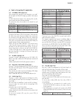
構成名
FILE 名(? 部分はバージョン依存)
バージョン
書き込み行程 [対象]
MAIN FIRMWARE
MCLP?̲??.PGM
V1.xx
CPU シート検査/
総合検査
[USB ストレージ]
サービス検査用 PC アプリ
¥TestProgram¥Service Test PC App
¥CLTest̲service.exe
V1.0.0
[検査用 PC]
DME-N Network Driver
¥TestProgram
¥DME‑N Network Driver v1.2.2¥Setup.exe
V1.2.2
[検査用 PC]
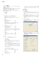
b. 本テストプログラムは OS: Windows 2000/XP/7 にて使用します。
サービス検査用 PC アプリを利用します。
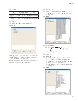
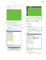
起動直後は Fig. 1 の画面となります。
起動画面(Fig. 1)
画面を閉じます(ツールバーに入ります)
このプログラムの終了
このプログラムの終了
(右上のボタンと同じ)
通信ポート(Ethernet
MIDI)の選択
ボタンをクリックすると
検査画面(Fig.2)となります
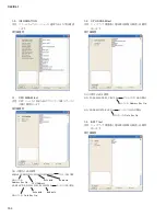
■ サービス検査プログラム
2-5. Fader Travel Time Measurement Test
Before this test, check to make sure that “FADER
CALIBRAION” on page 170 has been executed.
Press any 3 switches simultaneously in the Encoder Input Test
mode, and the Fader Travel Time Measurement Test mode will
be activated.
First, repeat reciprocal movement of all faders by the speci
fi
ed
number of times before taking measurement.
The check results are indicated with SEL/ON LEDs arranged
on each fader.
If ascending is NG,the SEL-LED turns on and if descending is
NG, the ON-LED turns on.
• Check to make sure that SEL/ON LEDs arranged on each
fader are all turned off.
It is possible to re-check by pressing whichever one switch.
2-6. All LEDs Lighting Test
Press any 3 switches simultaneously in the CH NAME LCD
display check mode, and the All LEDs Lighting Test mode will
be activated.
Con
fi
rm visually that all LEDs on the panel are turned on.
Summary of Contents for CL3
Page 7: ...7 CL3 CL1 DIMENSIONS CL3 CL1 648 15 201 130 299 667 839 15 201 130 299 667 Unit mm...
Page 95: ...95 CL3 CL1 CPU Circuit Board Pattern side to DSP CN101 2NA WY67750 1...
Page 101: ...101 CL3 CL1 DNTU Circuit Board Pattern side Scale 80 100 2NA WZ20390 5...
Page 102: ...CL3 CL1 102 2NA WY63530 FX Circuit Board WR 63 1 Component side Scale 95 100...
Page 103: ...103 CL3 CL1 2NA WY63530 FX Circuit Board Pattern side Scale 95 100...
Page 105: ...105 CL3 CL1 HAAD Circuit Board Pattern side Scale 90 100 2NA WY64340 2...
Page 107: ...107 CL3 CL1 2NA WY63490 Component side JK Circuit Board WR 63 1...
Page 109: ...109 CL3 CL1 Component side TBPHN Circuit Board WR 06 1 WR 63 1 2NA WY64360 1...
Page 110: ...CL3 CL1 110 Component side PN8 Circuit Board to FD8 CN902 or FD8CN CN902 2NA WY53120 2...
Page 118: ...CL3 CL1 118 Component side PNENL Circuit Board to PN8 CN001 2NA WY53130 1...
Page 160: ...CL3 CL1 160 1 18 LCD Test LCD LCD 1 3 2 9 5 OK NG 1 2 H 3 O X O 4 BOX 5x4...
Page 382: ...7 MBCL CIRCUIT BOARDS A A A A 2NA WY53200 1 MB Circuit Board Component side...
Page 383: ...MBCL 8 MB Circuit Board DSUB PH CONNECTOR ASSEMBLY B B B B 2NA WY53200 1 Pattern side...


